background image

27 

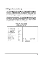
4.4 Chipset Features Setup 

This section allows you to configure the system based on the specific 
features of the installed chipset. This chipset manages bus speeds 
and the access to the system memory resources, such as DRAM and 
the external cache.  It also coordinates the communications between 
the conventional ISA and PCI buses. It must be stated that these 
items should never be altered. The default settings have been chosen 
because they provide the best operating conditions for your system. 
You might consider and make any changes only if you discover that 
the data has been lost while using your system. 


ROM PCI/ISA BIOS (2A59GD3G) 

CHIPSET FEATURES SETUP  

AWARD SOFTWARE, INC.  

Auto Configuration 

:  Enabled 

Delayed Transaction 

Disabled 


:   


DRAM RAS# Precharge Time 

:  3 


DRAM R/W Leadoff Timing 

:  7 


Fast RAS To CAS Delay  

:  3 


DRAM Read Burst (EDO/FP) 

:  x444/x444 


DRAM Write Burst Timing 

:  x444 


Fast MA to RAS# Delay CLK 

:  2 


Fast EDO Path Select 

:  Disabled 


Refresh RAS# Assertion 

:  4 Clks 


ISA Bus Clock 

:  PCI CLK/4 


SDRAM (CAS Lat/RAS-to-CAS) 

:  3/3 


System BIOS Cacheable  

:  Disabled 


Video BIOS Cacheable  

:  Disabled 


8 Bit I/O Recovery Time 

:  1 


16 Bit I/O Recovery Time 

:  1 

ESC 

: Quit 

????

: Select Item 

Memory Hole At 15M-16M 

:  Disabled 

F1 

: Help 

PU/PD/+/-: Modify  

Peer Concurrency  

:  Disabled 

F5 

: Old Values 

(Shift) F2  : Color 

Passive Release  

  Disabled 

F6 

: Load BIOS Defaults 


F7 

: Load Setup Defaults 


Содержание HS-5010

Страница 1: ...HS 5010 Pentium VGA I S B Full Size TritonTM VX All in one PICMGTM Bus Industrial Single Board Computer...

Страница 2: ...ge the contents of this manual without prior notices in order to improve the function design performance quality and reliability The author assumes no responsibility for any errors or omissions which...

Страница 3: ...PCI VGA CONTROLLER 14 2 8 DISKONCHIP ADDRESS SETTING 14 2 9 CPU TEMPERATURE ALARM 12 CONNECTION 15 3 1 FLOPPY DISK DRIVE CONNECTOR 15 3 2 PCI E IDE DRIVE CONNECTOR 16 3 3 PARALLEL PORT 17 3 4 SERIAL...

Страница 4: ...ii Contents AWARD BIOS SETUP 22 4 1 MAIN MENU 23 4 2 STANDARD CMOS SETUP 24 4 3 BIOS FEATURES SETUP 25 4 4 CHIPSET FEATURES SETUP 26 4 5 INTEGRATED PERIPHERALS 27 4 6 POWER MANAGEMENT SETUP 28...

Страница 5: ...using S3 86C775 chipset with 2MB memory The HS 5010 takes advantage of both 32bit PCI and 16bit ISA bus to provide high performance graphics accelerator VGA resolution is supported up to 1024 by 768...

Страница 6: ...peline burst cache memory Floppy Disk Drive Interface Supports up to two floppy disk drives Parallel Port One bi directional parallel port Supports SPP ECP EPP mode Serial Port Two RS 232 ports Both u...

Страница 7: ...n 13 26 L x 4 8 W 337mm x 122mm 1 2 What do you have The HS 5010 package includes the following items HS 5010 Industrial Single Board Computer Printer port flat cable IDE port flat cable FDD port flat...

Страница 8: ...6 2 1 HS 5010 s Layout...

Страница 9: ...ti static mat The operator should be wearing an anti static wristband grounded at the same point as the anti static mat Be sure that there are no shipping and handling damages on the board before unpa...

Страница 10: ...nfiguration please follow the instructions A jumper switch is closed sometimes referred to as shorted with a plastic cap inserted over two pins of the jumper A jumper is open with a plastic cap insert...

Страница 11: ...specification Please reference to the following table for all type CPU in used CPU s Clock Ratio Select Clock Ratio BF2 BF1 BF0 Intel AMD JP9 JP13 JP12 P54C P55C K6 1 2 1 2 1 2 2 5 2 5 2 5 OFF ON ON 3...

Страница 12: ...all CPU operating User may selected from 2 8V to 3 5V CPU Voltage JP6 2 8V 7 8 2 9V 5 6 3 2V All Open 3 3V 1 2 3 5V 3 4 default setting CPU Clock in Select JP10 50MHz 1 2 3 4 55MHz 1 2 3 4 60MHz 3 4 5...

Страница 13: ...11 Refresh Based JP14 60MHz ON 66MHz OFF default setting Sysclk Configuration JP15 Divided by 4 ON Divided by 3 OFF default setting...

Страница 14: ...ram operation is abnormal and will either issue a reset signal to start again or activate a NMI to the CPU The Watch Dog Timer is disabled by reading the port 043H JP23 determines the Watch Dog Timer...

Страница 15: ...Dog timer will automatically reset the system or issue a NMI Non maskable interrupt The Watch Dog Timer is controlled by two I O ports 443H I O Read Enable refresh the Watch Dog Timer 043H I O Read D...

Страница 16: ...14 IN AL DX POP DX get back AX DX POP AX RET...

Страница 17: ...get more VGA drivers information please refer to the S3 Internet address www s3 com 2 8 DiskOnChipTM Address Setting Install the DiskOnChipTM in U21 socket Please select the memory address JP18 DiskOn...

Страница 18: ...nnector PIN NO DESCRIPTION PIN NO DESCRIPTION 1 GROUND 2 REDUCE WRITE 3 GROUND 4 N C 5 GROUND 6 N C 7 GROUND 8 INDEX 9 GROUND 10 MOTOR ENABLE A 11 GROUND 12 DRIVE SELECT B 13 GROUND 14 DRIVE SELECT A...

Страница 19: ...IDE Interface Connector PIN NO DESCRIPTION PIN NO DESCRIPTION 1 RESET 2 GROUND 3 DATA 7 4 DATA 8 5 DATA 6 6 DATA 9 7 DATA 5 8 DATA 10 9 DATA 4 10 DATA 11 11 DATA 3 12 DATA 12 13 DATA 2 14 DATA 13 15 D...

Страница 20: ...R SELECT 14 AUTO FORM FEED 15 ERROR 16 INITIALIZE 17 PRINTER SELECT LN 18 GROUND 19 GROUND 20 GROUND 21 GROUND 22 GROUND 23 GROUND 24 GROUND 25 GROUND 26 GROUND 3 4 Serial Ports The HS 5010 offers two...

Страница 21: ...DTR 8 RI 9 GND 10 NC 3 5 Keyboard Connector The HS 5010 provides two keyboard connector CN1 5pin Header Keyboard Connector PIN NO Description 1 Keyboard Clock 2 Keyboard Data 3 N C 4 Ground 5 5V CN13...

Страница 22: ...ion 1 Power LED Anode 2 Key 3 Ground 4 Keylock 5 Ground JP1 Reset Button PIN NO Description 1 External Reset 2 Ground JP3 IDE LED Connector PIN NO Description 1 5V 2 HDD Active 3 7 External Speaker Th...

Страница 23: ...IRQ12 JP16 Description Open No Interrupt for PS 2 Close IRQ12 default setting CN11 PS 2 Mouse Connector PIN NO Description 1 MS Data 2 N C 3 Ground 4 5V 5 KBT1 6 N C 3 9 VGA Connector The HS 5010 has...

Страница 24: ...d 3 11 Internal VGA Connector CN8 10 pin Internal VGA Connector PIN NO Description PIN NO Description 1 Red 2 Ground 3 Green 4 Ground 5 Blue 6 Ground 7 HSYNC 8 Ground 9 VSYNC 10 Ground 3 12 IR Connect...

Страница 25: ...is designed to provide the maximum flexibility in configuring the system by offering various options which could be selected for end user requirements This chapter is written to assist you in the prop...

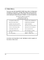
Страница 26: ...IOS 2A59GD3G CMOS SETUP UTILITY AWARD SOFTWARE INC STANDARD CMOS SETUP BIOS FEATURES SETUP CHIPSET FEATURES SETUP POWER MANGEMENT SETUP PNP PCI CONFIGURATION LOAD BIOS DEFAULTS LOAD SETUP DEFAULTS INT...

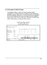
Страница 27: ...he IDE Setup Utility in BIOS Setup to install the HDD correctly ROM PCI ISA BIOS 2A59GD3G STANDARD CMOS SETUP AWARD SOFTWARE INC Data mm dd yy Fri Oct 19 1999 Time hh mm ss 00 00 00 CYLS HEAD PRECOMP...

Страница 28: ...Shadow Disabled Quick Power On Self Test Disabled D0000 D3FFF Shadow Disabled Boot Sequence A C SCSI D4000 D7FFF Shadow Disabled Swap Floppy Drive Disabled D8000 DBFFF Shadow Disabled Boot Up Floppy S...

Страница 29: ...the data has been lost while using your system ROM PCI ISA BIOS 2A59GD3G CHIPSET FEATURES SETUP AWARD SOFTWARE INC Auto Configuration Enabled Delayed Transaction Disabled DRAM RAS Precharge Time 3 DRA...

Страница 30: ...fer to or from the disk drive PIO allows the BIOS to tell the controller what it wants and then let the controller and the CPU perform the complete task by them This is much simpler and more efficient...

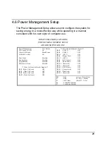
Страница 31: ...Blank Screen IRQ4 COM 1 OFF MODEM Use IRQ NA IRQ5 LPT 2 OFF IRQ6 Floppy Disk OFF Doze Mode Disabled IRQ7 LPT 1 OFF Standby Mode Disabled IRQ8 RTC Alarm OFF Suspend Mode Disabled IRQ9 IRQ2 Redir OFF H...

Отзывы: