background image

User’s Manual

BOSCH

- 35/77 -

Revision 1.6

TTCAN

 11.11.02

manual_about.fm

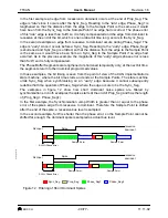
 3.5.13 TT Cycle Count Register (addresses 0x3D & 0x3C)

C_Cnt5-0

Cycle_Count

0x00-0x3F

The number of the actual Basic Cycle in the System Matrix.

 3.5.14 TT Error Level Register (addresses 0x3F & 0x3E)

MSCmax

Maximum Message Status Count

0x0-0x7

The highest Message Status Count of all periodic Message Objects.

MSCmin

Minimum Message Status Count

0x0-0x7

The lowest Message Status Count of all periodic Message Objects.

TTEL

TT Error Level

0x0

severity 0 : No Error

0x1

severity 1 : Warning

0x2

severity 2 : Error

0x3

severity 3 : Fatal Error

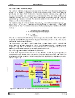
 3.5.15 TUR Numerator Configuration Low Register (addresses 0x57 & 0x56)

NumCfgL TUR Numerator Configuration (low part)

0x0000-0xFFFF

NumCfg[15

0]

NumCfg is an 18-bit value. Its high part, NumCfg[17

16] is hard wired to 0b01. The range of

NumCfg is [0x10000

0x1FFFF]. The value configured in NumCfg is the initial value for

NumAct, so when the number 0xnnnn is written to NumCfg[15

0], NumAct starts with the

value 0x1nnnn. NumCfgL may be written during Configuration Mode or if EESC (Enable
External Clock Synchronisation) is set. When a new value for NumCfgL is written after
Configuration Mode, the new value takes effect when the ECS bit of the TT Clock Control
register is written to ‘1’.

Note : The actual value of TUR may be changed by the clock drift compensation function of TTCAN

Level 2 in order to adjust the node’s local view of the NTU to the time master view of the NTU.
DenomCfg will not be changed by the automatic drift compensation, NumAct may be adjusted
in the range of the Synchronisation Deviation Limit around NumCfgNumCfg and DenomCfg
should be programmed to the largest suitable values in order to allow the best computational
accuracy for the drift compensation process.

15

14

13

12

11

10

9

8

7

6

5

4

3

2

1

0

reserved

res

C_Cnt5-0

r

r

r

15

14

13

12

11

10

9

8

7

6

5

4

3

2

1

0

reserved

MSCmax

MSCmin

TTEL

r

r

r

r

15

14

13

12

11

10

9

8

7

6

5

4

3

2

1

0

NumCfgL

rw

rw

Содержание TTCAN

Страница 1: ...ual BOSCH Revision 1 6 TTCAN 11 11 02 manual_about fm Robert Bosch GmbH Automotive Electronics Semiconductors and Integrated Circuits Digital CMOS Design Group TTCAN IP Module User s Manual Revision 1 6 11 11 02 ...

Страница 2: ...eans electronic mechanical manual optical or otherwise without prior written permission of Robert Bosch GmbH or as expressly provided by the license agreement Disclaimer ROBERT BOSCH GMBH MAKES NO WARRANTY OF ANY KIND EXPRESS OR IMPLIED WITH REGARD TO THIS MATERIAL INCLUDING BUT NOT LIMITED TO THE IMPLIED WARRANTIES OF MERCHANTABILITY AND FITNESS FOR A PARTICULAR PURPOSE ROBERT BOSCH GMBH RESERVES...

Страница 3: ...3 2 3 4 6 Software control of Pin CAN_TX 14 2 3 4 7 No Message RAM Mode 14 3 Programmer s Model 15 3 1 Hardware Reset Description 16 3 2 CAN Protocol Related Registers 17 3 2 1 CAN Control Register addresses 0x01 0x00 17 3 2 2 Status Register addresses 0x03 0x02 18 3 2 2 1 Status Interrupts 19 3 2 3 Error Counter addresses 0x05 0x04 19 3 2 4 Bit Timing Register addresses 0x07 0x06 19 3 2 5 BRP Ext...

Страница 4: ...rator Configuration Low Register addresses 0x57 0x56 35 3 5 16 TUR Denominator Configuration Register addresses 0x59 0x58 36 3 5 17 TUR Numerator Actual Registers addresses 0x5B 0x5A 36 3 5 18 TT Stop_Watch Register addresses 0x61 0x60 36 3 5 19 TT Global Time Preset Register addresses 0x65 0x64 37 3 5 20 TT Clock Control Register addresses 0x67 0x66 37 3 5 21 TT Sync_Mark Register addresses 0x69 ...

Страница 5: ...cation 60 5 1 TTCAN Configuration 60 5 1 1 TTCAN Timing 60 5 1 2 Message Scheduling 61 5 1 3 Trigger Memory 62 5 1 4 Message Objects 64 5 1 4 1 Reference Message 64 5 1 4 2 Periodic Transmit Message 64 5 1 4 3 Event Driven Transmit Message 65 5 2 TTCAN Schedule Initialisation 65 5 2 1 Time Slaves 65 5 2 2 Potential Time Masters 65 5 3 TTCAN Message Handling 66 5 3 1 Message Reception 66 5 3 2 Mess...

Страница 6: ...Editorial changes Revision 1 6 11 11 02 F Hartwich Watchdog Gap Control Global Time Preset 1 2 Conventions The following conventions are used within this User s Manual Helvetica bold Names of bits and signals Helvetica italic States of bits and signals 1 3 Scope This document describes the TTCAN IP module and its features from the application programmer s point of view All information necessary to...

Страница 7: ...s the following terms and abbreviations Term Meaning CAN Controller Area Network BSP Bit Stream Processor BTL Bit Timing Logic CRC Cyclic Redundancy Check Register DLC Data Length Code EML Error Management Logic FSE Frame Synchronisation Entity FSM Finite State Machine NTU Network Time Unit TTCAN Time Triggered CAN ...

Страница 8: ...he Message RAM The time triggers defining the transmission schedule are stored in the Trigger RAM All functions concerning the handling of messages are implemented in the Message Handler Those functions are acceptance filtering transfer of messages between the CAN_Core and the Message RAM and the handling of transmission requests as well as the generation of the module interrupt All functions conc...

Страница 9: ... machine that controls the ISO 11898 4 time triggered communication It synchronises itself to the reference messages on the CAN bus controls Cycle Time and Global Time and handles transmissions according to the predefined message schedule the system matrix StopWatch Trigger EVent Trigger and Time Mark Interrupt are synchronisation interfaces The Trigger Memory stores the time marks of the system m...

Страница 10: ...the configuration of a Message Object during normal operation the CPU has to start by setting MsgVal to not valid When the configuration is completed MsgVal is set to valid again To change the configuration of the time triggered communication the TTMode in the TT Operation Mode Register must be set to Configuration Mode Entering and leaving this Configuration Mode requires that both bits Init and ...

Страница 11: ...essage Buffer is reset while bit NewDat remains set When the transmission completed successfully bit NewDat is reset When a transmission failed lost arbitration or error bit NewDat remains set To restart the transmission the CPU has to set TxRqst back to one Note It is not necessary to set DAR if the TTCAN is in time triggered operating mode 2 3 4 Test Mode The Test Mode is entered by setting bit ...

Страница 12: ...the TTCAN is in time triggered operating mode if the TTCAN is in event driven CAN mode WdOff is remains set and the TT Application Watchdog remains disabled emulating the C_CAN function The TT Application Watchdog should not be disabled in a TTCAN application program 2 3 4 3 Silent Mode The CAN_Core can be set in Silent Mode by programming the Test Register bit Silent to one In Silent Mode the TTC...

Страница 13: ... mode the CAN_Core performs an internal feedback from its Tx output to its Rx input The actual value of the CAN_RX input pin is disregarded by the CAN_Core The transmitted messages can be monitored at the CAN_TX pin 2 3 4 5 Loop Back combined with Silent Mode It is also possible to combine Loop Back Mode and Silent Mode by programming bits LBack and Silent to one at the same time This mode can be ...

Страница 14: ...put signal CAN_WAIT_B is disabled always 1 in this mode As soon the CAN bus is idle the IF1 Registers are loaded into the CAN_Core s shift register and the transmission is started When the transmission has completed the Busy bit is reset and the locked IF1 Registers are released A pending transmission can be aborted at any time by resetting the Busy bit in the IF1 Command Request Register while th...

Страница 15: ...ask 1 0xFFFF CAN Base 0x16 IF1 Mask 2 0xFFFF CAN Base 0x18 IF1 Arbitration 1 0x0000 CAN Base 0x1A IF1 Arbitration2 0x0000 CAN Base 0x1C IF1 Message Control 0x0000 CAN Base 0x1E IF1 Data A 1 0x0000 CAN Base 0x20 IF1 Data A 2 0x0000 CAN Base 0x22 IF1 Data B 1 0x0000 CAN Base 0x24 IF1 Data B 2 0x0000 CAN Base 0x26 reserved 2 CAN Base 0x28 TT Operation Mode 0x0000 TTCAN config register CAN Base 0x2A T...

Страница 16: ...tL 0x0000 TTCAN status register CAN Base 0x5C TUR NumeratorActH 0x0001 TTCAN status register CAN Base 0x5E reserved 2 CAN Base 0x60 Stop_Watch 0x0000 TTCAN status register CAN Base 0x62 reserved 2 CAN Base 0x64 Global Time Preset 0x0000 TTCAN appl register CAN Base 0x66 Clock Control 0x1000 TTCAN appl register CAN Base 0x68 Sync_Mark 0x0000 TTCAN status register CAN Base 0x6A reserved 2 CAN Base 0...

Страница 17: ...e Interrupt Enable one Enabled Interrupts will set IRQ_B to LOW IRQ_B remains LOW until all pending interrupts are processed zero Disabled Module Interrupt IRQ_B is always HIGH Init Initialization one Initialization is started zero Normal Operation The configuration registers controlled by CCE are the Bit Timing Register the BRP Extension Register and the TT Operation Mode Register Note The Bus_Of...

Страница 18: ... CAN bus 0 No Error 1 Stuff Error More than 5 equal bits in a sequence have occurred in a part of a received message where this is not allowed 2 Form Error A fixed format part of a received frame has the wrong format 3 AckError The message this CAN Core transmitted was not acknowledged by another node 4 Bit1Error During the transmission of a message with the exception of the arbitration field the ...

Страница 19: ...04 RP Receive Error Passive one The Receive Error Counter has reached the error passive level as defined in the CAN Specification zero The Receive Error Counter is below the error passive level REC6 0 Receive Error Counter Actual state of the Receive Error Counter Values between 0 and 127 TEC7 0 Transmit Error Counter Actual state of the Transmit Error Counter Values between 0 and 255 3 2 4 Bit Ti...

Страница 20: ...n its default width of 4 bits in particular imple mentations of the TTCAN IP module width a high module clock frequency 3 3 Message Interface Register Sets Figure 6 IF1 and IF2 Message Interface Register Sets There are two sets of Interface Registers that control the CPU access to the Message RAM The Interface Registers avoid by buffering the data to be transferred conflicts between CPU access to ...

Страница 21: ...e Object in the Message RAM as target or source for the transfer and to start the action specified in the Command Mask Register 3 3 1 IFx Command Mask Registers The control bits of the IFx Command Mask Register specify the transfer direction and select which of the IFx Message Buffer Registers are source or target of the data transfer WR RD Write Read one Write Transfer data from the selected Mess...

Страница 22: ... Bits to IFx Message Buffer Register zero Control Bits unchanged ClrIntPnd Clear Interrupt Pending Bit one clear IntPnd bit in the Message Object zero IntPnd bit remains unchanged TxRqst NewDatAccess New Data Bit one clear NewDat bit in the Message Object zero NewDat bit remains unchanged Note A read access to a Message Object can be combined with the reset of the control bits IntPnd and NewDat Th...

Страница 23: ... Note When an invalid Message Number is written to the Command Request Register the Message Number will be transformed into a valid value and that Message Object will be transferred 3 3 3 IFx Message Buffer Registers The bits of the Message Buffer registers mirror the Message Objects in the Message RAM The function of the Message Objects bits is described in chapter 3 3 4 3 3 3 1 IFx Mask Register...

Страница 24: ...et before the iden tifier Id28 0 the control bits Xtd Dir or the Data Length Code DLC3 0 are modified or if the Messages Object is no longer required UMask Use Acceptance Mask one Use Mask Msk28 0 MXtd and MDir for acceptance filtering zero Mask ignored Note If the UMask bit is set to one the Message Object s mask bits have to be programmed during initialization of the Message Object before MsgVal...

Страница 25: ...e direction bit Dir is used for acceptance filtering zero The message direction bit Dir has no effect on the acceptance filtering The Arbitration Registers ID28 0 Xtd and Dir are used to define the identifier and type of outgoing messages and are used together with the mask registers Msk28 0 MXtd and MDir for acceptance filtering of incoming messages A received message is stored into the valid Mes...

Страница 26: ...bject if there is no other interrupt source with higher priority zero This message object is not the source of an interrupt RmtEn Remote Enable one At the reception of a Remote Frame TxRqst is set zero At the reception of a Remote Frame TxRqst is left unchanged TxRqst Transmit Request one The transmission of this Message Object is requested and is not yet done zero This Message Object is not waiti...

Страница 27: ...9 0x08 IntId15 0 Interrupt Identifier the number here indicates the source of the interrupt 0x0000 No interrupt is pending 0x0001 0x0020 Number of Message Object which caused the interrupt 0x0021 0x3FFF unused 0x4000 TTCAN Interrupt 0x4001 0x7FFF unused 0x8000 Status Interrupt 0x8001 0xBFFF unused 0xC000 TTCAN Interrupt and Status Interrupt 0xC001 0xFFFF unused If several interrupts are pending th...

Страница 28: ...on was updated The NewDat bit of a specific Message Object can be set reset by the CPU via the IFx Message Interface Registers or by the Message Handler after reception of a Data Frame or after a successful transmission 3 4 4 Interrupt Pending Registers IntPnd32 1 Interrupt Pending Bits of all Message Objects one This message object is the source of an interrupt zero This message object is not the...

Страница 29: ...Memory access is started by a write to the low byte of the Trigger Memory Access register 3 5 2 IF1 Data B1 and B2 Registers for Trigger Memory Access The trigger data of the TTCAN system matrix is stored in the Trigger Memory The Trigger Memory is accessed via the IF1 Data B1 and B2 Registers The data transfer is controlled by the Trigger Memory Access Register The bits of IF1 Data B1 and B2 Regi...

Страница 30: ...001cccc valid every sixteenth Cycle at Cycle_Count mod 16 cccc 0b01ccccc valid every thirty second Cycle at Cycle_Count mod 32 ccccc 0b1cccccc valid every sixty fourth Cycle at Cycle_Count mod 64 cccccc Time_Mark 0x0000 0xFFFF Cycle Time for which the trigger becomes active Note The Message Number must be 1 for Type Tx_Ref_Trigger and Tx_Ref_Trigger_Gap The Message Number is not regarded for Type ...

Страница 31: ...sters require TTMode_1 Configuration Mode to be writable 3 5 4 TT Matrix Limits1 Register addresses 0x2B 0x2A ETT Expected Tx_Trigger 0x000 0xfFF Expected number of Tx_Triggers in one matrix cycle 3 5 5 TT Matrix Limits2 Register addresses 0x2D 0x2C RDLC Reference Message Data Length Code 0x0 invalid value 0x1 0xF DLC of Reference Message to transmit when Time Master TEW Tx_Enable Window 0x0 0xF L...

Страница 32: ...sabled by programming the Test Register bit WdOff to 1 and AppWdL to 0x00 see chapter 2 3 4 2 3 5 7 TT Interrupt Enable Register addresses 0x31 0x30 There is for each bit in the TT Interrupt Vector register one corresponding enable bit in the TT Interrupt Enable register 1 meaning enabled and 0 meaning disabled The TT Interrupt Vector register bits will be updated regardless of the TT Interrupt En...

Страница 33: ...ted_Tx_Trigger in one Matrix Cycle GTE Global Time Error Set when Synchronisation Deviation SD exceeds specified limit SDL level2 only Dis Global Time Discontinuity Set on discontinuity of the Global Time Disc_Bit in the Reference Message GTW Global Time Wrap Set when a Global Time wrap occurred from 0xFFFF to 0x0000 SWE Stop Watch Event Set when a rising edge is detected at the STOP_WATCH_TRIGGER...

Страница 34: ...de waits for event triggered Reference Message zero The node does not wait for event triggered Reference Message TMP2 0 Time Master Priority 0x0 0x7 The priority of the actual Time Master SyncSt TTCAN Synchronisation State 0x0 Out of Synchronisation 0x1 Synchronising to TTCAN communication 0x2 In_Gap Schedule suspended by Gap 0x3 In_Schedule Synchronised to Schedule MState TTCAN Master State and O...

Страница 35: ...g is the initial value for NumAct so when the number 0xnnnn is written to NumCfg 15 0 NumAct starts with the value 0x1nnnn NumCfgL may be written during Configuration Mode or if EESC Enable External Clock Synchronisation is set When a new value for NumCfgL is written after Configuration Mode the new value takes effect when the ECS bit of the TT Clock Control register is written to 1 Note The actua...

Страница 36: ...F NumAct 17 0 0x21000 invalid value There is no drift compensation in TTCAN Level 1 NumAct NumCfg In TTCAN Level 2 the drift between local clock and the time master s local clock is calculated The drift is compensated when the Synchronisation Deviation difference between NumCfg and the calculated new NumAct is not more than 2 ldSDL 5 With ldSDL 7 this results in a maximum range for NumAct of NumCf...

Страница 37: ...eviation 2 ldSDL 5 QCS Quality of Clock Speed one SD SDL always true in TTCAN Level 1 zero Local clock speed not synchronised to Time Master clock speed QGTP Quality of Global Time Phase one Global Time in phase with Time Master zero Global Time not valid always true in TTCAN Level 1 ECAL Enable Clock Calibration one The automatic clock calibration in TTCAN Level2 is enabled zero The automatic clo...

Страница 38: ...er SGT has been set by the CPU GTDiff is locked while WGTD is set zero No Global Time Preset is pending SGT Set Global Time The Global Time Preset takes effect when 1 is written to SGT SGT will always be read as 0 The Synchronisation Deviation SD is the difference between NumCfg and NumAct When the calculated NumAct deviates by more than 2 ldSDL 5 from NumCfg the drift compensation is suspended an...

Страница 39: ...1 zero The bit is reset automatically at each Reference Message Gap Now is Gap one The Gap time after the Basic Cycle has started and TTMODE_3 zero No Gap in Schedule this bit is reset automatically at each Refer ence Message and in nodes that are time slaves GpH Gap Herald one Next_is_Gap 1 in Reference Message and TTMODE_3 zero No Gap announced this bit is reset automatically at each Refer ence ...

Страница 40: ...y the CPU directely Another method to set FGp is using the TMI interrupt When TMG is set to 1 the next TMI will set FGp The third way to set FGp is using the EVENT_TRIGGER input pin When EPE is set to 1 an edge from high to low at the EVENT_TRIGGER will set FGp When FGp is set after the Gap time has started that event will start the transmission of a Reference Message immediately and will thereby ...

Страница 41: ...age RAM received messages Handling of TxRqst flags Handling of interrupts 4 1 1 Data Transfer Between IFx Registers and Message RAM There are two sets of IFx Registers Each set of IFx Registers consists of Command Registers controlling the data transfer and Message Buffer Registers containing the Message Object The Command Request Register addresses the desired Message Object in the Message RAM th...

Страница 42: ...ge Object with the highest priority pending transmission request is loaded into the shift register by the Message Handler and the transmission is started The Message Object s NewDat bit is reset After a successful transmission and if no new data was written to the Message Object NewDat 0 since the start of the transmission the TxRqst bit will be reset If TxIE is set IntPnd will be set after a succ...

Страница 43: ...n it reads the Message Object If at the time of the reception the NewDat bit was already set MsgLst is set to indicate that the previous data supposedly not seen by the CPU is lost If the RxIE bit is set the IntPnd bit is set causing the Interrupt Register to point to this Message Object The TxRqst bit of this Message Object is reset to prevent the transmission of a Remote Frame while the requeste...

Страница 44: ...r is set additionally to Init This is not required for the configuration of the Message Objects The configuration of the TTCAN functions see chapter 5 requires that TTMode is set to Configuration Mode The bits MsgVal NewDat IntPnd and TxRqst of the Message Objects are reset to 0 by the hardware reset the other contents of the Message RAM are not affected by a hardware reset The configuration of a ...

Страница 45: ...erature or voltage and by deteriorating components As long as the variations remain inside a specific oscillator tolerance range df the CAN nodes are able to compensate for the different bit rates by resynchronising to the bit stream According to the CAN specification the bit time is divided into four segments see figure 9 The Synchronisation Segment the Propagation Time Segment the Phase Buffer S...

Страница 46: ...le both nodes A and B are transmitters performing an arbitration for the CAN bus The node A has sent its Start of Frame bit less than one bit time earlier than node B therefore node B has synchronised itself to the received edge from recessive to dominant Since node B has received this edge delay A_to_B after it has been transmitted B s bit timing segments are shifted with regard to A Node B sends...

Страница 47: ... to compensate for the oscillator tolerance The Phase Buffer Segments may be lengthened or shortened by synchronisation Synchronisations occur on edges from recessive to dominant their purpose is to control the distance between edges and Sample Points Edges are detected by sampling the actual bus level in each time quantum and comparing it with the bus level at the previous Sample Point A synchron...

Страница 48: ...itter does not necessarily win the arbitration therefore the receivers have to synchronise themselves to different transmitters that subsequently take the lead and that are differently synchronised to the previously leading transmitter The same happens at the acknowledge field where the transmitter and some of the receivers will have to synchronise to that receiver that takes the lead in the trans...

Страница 49: ...Segments are lengthened or shortened temporarily only at the next bit time the segments return to their nominal programmed values In these examples the bit timing is seen from the point of view of the CAN implementation s state machine where the bit time starts and ends at the Sample Points The state machine omits Sync_Seg when synchronising on an early edge because it cannot subsequently redefine...

Страница 50: ...Time Segment limits that part of the bit time that may be used for the Phase Buffer Segments The combination Prop_Seg 1 and Phase_Seg1 Phase_Seg2 SJW 4 allows the largest possible oscillator tolerance of 1 58 This combination with a Propagation Time Segment of only 10 of the bit time is not suitable for short bit times it can be used for bit rates of up to 125 kBit s bit time 8 µs with a bus lengt...

Страница 51: ...ulate the next bit to be sent e g data bit CRC bit stuff bit error flag or idle is called the Information Processing Time IPT The IPT is application specific but may not be longer than 2 tq the TTCAN s IPT is 0 tq Its length is the lower limit of the programmed length of Phase_Seg2 In case of a synchronisa tion Phase_Seg2 may be shortened to a value less than IPT which does not affect bus timing 4...

Страница 52: ...lity has to be increased in order to find a protocol compliant configuration of the CAN bit timing The resulting configuration is written into the Bit Timing Register Phase_Seg2 1 Phase_Seg1 Prop_Seg 1 SynchronisationJumpWidth 1 Prescaler 1 4 2 1 7 Example for Bit Timing at high Baudrate In this example the frequency of CAN_CLK is 10 MHz BRP is 0 the bit rate is 1 MBit s tq 100 ns tCAN_CLK delay o...

Страница 53: ... and IntPnd Read received data Get the complete message from a Message Object and clear NewDat and IntPnd Read a received message including identifier from a Message Object with UMask 1 Parameters of the subroutines are the Message Number and a pointer to a complete message structure or to the data bytes of a message structure Two methods are possible to assign the IFx Interface Register sets to t...

Страница 54: ...ransmission of a Data Frame 4 2 2 1 Configuration of a Transmit Object for Data Frames Figure 14 shows how a Transmit Object should be initialised Figure 14 Initialisation of a Transmit Object The Arbitration Registers ID28 0 and Xtd bit are given by the application They define the identifier and type of the outgoing message If an 11 bit Identifier Standard Frame is used Xtd 0 it is programmed to ...

Страница 55: ...ts belonging to a FIFO Buffer is the same as the configuration of a single Receive Object see section 4 2 2 2 To concatenate two or more Message Objects into a FIFO Buffer the identifiers and masks if used of these Message Objects have to be programmed to matching values Due to the implicit priority of the Message Objects the Message Object with the lowest number will be the first Message Object o...

Страница 56: ...s is used only for reading of received messages its Command Mask Register may be kept constant at 0x7F meaning that always the whole Message Object is transferred into the Interface Register set NewDat and IntPnd are reset To update the data bytes of a message to be transmitted the Command Mask Register should be set to 0x87 all transmit messages in C_CAN emulation mode or event triggered message ...

Страница 57: ...nterrupt service routine to analyse the CAN bus errors AckError e g indicates that no other node is active on the CAN bus The CPU has two possibilities to follow the source of a message interrupt First it can follow the IntId in the Interrupt Register and second it can poll the Interrupt Pending Register see section 3 4 4 An interrupt service routine reading the message that is the source of the i...

Страница 58: ...ssages has been received The actual value of NewDat shows whether a new message has been received since last time this Message Object was read The actual value of MsgLst shows whether more than one message has been received since last time this Message Object was read MsgLst will not be automatically reset 4 3 5 Requesting New Data for a Receive Object By means of a Remote Frame the CPU may reques...

Страница 59: ... case Interrupt Pointer 0x8000h else 0x0000h Status Change END IFx Command Mask 0x007F Write MessageNum to IFx Command Request Transfer Message to IFx Registers Clear NewDat and IntPnd Read IFx Message Control NewDat 1 Read Data from IFx Data A B EoB 1 MessageNum MessageNum 1 Yes No Yes No Message Interrupt Interrupt Handling MessageNum Interrupt Pointer ...

Страница 60: ...mAct within a specified limit in order to compensate for clock drift between their local clock and the time master s clock The Synchronisation Deviation SD NumCfg NumAct is limited by the Synchronisation Deviation Limit SDL which is configured by its dual logarithm ldSDL SDL 2 ldSDL 5 and should not exceed the clock tolerance given by the CAN bit timing configuration SD is calculated at each new B...

Страница 61: ... the master priority is identical to the three LSBs of the Reference Message Identifier MPr is not relevant for Time Slaves The Initial Reference Trigger Offset Init_Ref_Offset is a 7 bit value that defines in NTUs how long a backup Time Master waits before it starts the transmission of a Reference Message when a Reference Message is expected but the bus remains idle The recommended value for Init...

Страница 62: ...ndow s message the transmission cannot be started in that Time Window at all TEW has to be chosen with respect to the network s synchronisation quality and with respect to the relation between the length of the Time Windows and the length of the messages Which interrupt sources to enable in the TT Interrupt Enable register is application specific Write accesses to the Interrupt Enable register are...

Страница 63: ...erence Message is n NTU long then a Trigger with a Time_Mark n will never become active and will be treated as a Configuration Error Starting point of the Cycle Time is the Sample Point of the Reference Message s Start of Frame bit The next Reference Message is requested when Cycle Time reaches the Tx_Ref_Trigger s Time_Mark The CAN_Core reacts on the transmission request at the next Sample Point ...

Страница 64: ...atching the same Cycle_Count When the Time_Mark of an Rx_Trigger is placed near the Time_Mark of a Tx_Ref_Trigger and the Ref_Trigger_Offset causes a reversal of their sequential order measured in Cycle Time 5 1 4 Message Objects The Message Status Count MSC of each Message Object has to be initialised to 0 It can only be written in Configuration Mode The configuration of Receive Objects for Time ...

Страница 65: ...ad Tx_Ref_Trigger_Gap and Watch_Trigger_Gap until the first Reference Message decides whether a Gap is active 5 2 1 Time Slaves After configuration a Time Slave will ignore its Watch_Trigger and Watch_Trigger_Gap when it did not receive any message before reaching the Watch_Triggers When it reaches Initial_Watch_Trigger not part of the Trigger List defined as maximum of Cycle Time IWT in the Inter...

Страница 66: ...3 TTCAN Message Handling 5 3 1 Message Reception In TTCAN the handling of received message is the same as in Event driven CAN Communication see chapter 4 1 3 1 The message s MSC will be updated at the message s Rx_Trigger s and gives additional means to check whether the received data arrived on time 5 3 2 Message Transmission In TTCAN the handling of message to be transmitted is similar as in Eve...

Страница 67: ...oftware control writing FGp 1 or under Hardware control a low level at the EVENT_TRIGGER pin will restart the schedule The third option is a time triggered restart when the application program writes TMG 1 controlled by the Time Mark register Neither of these options can cause a Basic Cycle to be interrupted with a Reference Message Any Potential Time Master will finish a Gap when it reaches its T...

Страница 68: ...will use its own Local Time as Global Time The time master establishes its own local time as global time by transmitting its own Ref_Marks in the Reference Message as Master_Ref_Marks A node that receives a Reference Message calculates its Local_Offset to the Global Time by comparing see figure 19 their local Ref_Mark with the received Master_Ref_Mark The node s view of the Global Time is Local Ti...

Страница 69: ...cal clock speed is adjusted by first writing the newly calculated NumCfg value DenomCfg cannot be updated into the TUR Numerator Configuration register The new value takes effect by writing 1 to the ECS bit of the Clock Control register The Global Time phase is adjusted by first writing the phase offset into the Global Time Preset register The new value takes effect by writing 1 to the SGT bit of ...

Страница 70: ...ovide a means to synchronise the application program to the communication schedule 5 8 Configuration Example This is a configuration example for a TTCAN system consisting of three nodes M0 M1 and S0 operating in TTCAN level 2 at a bit rate of 1 MBit s All three nodes have a system clock frequency of 10 MHz the network time unit NTU is 1µs Two nodes M0 and M1 are potential time masters the third no...

Страница 71: ...ratorCfg 0x1FFFE clock periods 0x3333 NTU NTU 1 µs FFFE 14 58 TUR DenominatorCfg 3333 15 6C TT Time Mark generate TMI at Time Mark 0100 0200 0300 16 6E TT Gap Control disable gap functions 0000 17 12 IF1 Command Mask write Mask Arb Control Data 00F3 18 14 IF1 Mask1 3 LSB of 11 bit Reference Mes sage identifier masked FFFF 19 16 IF1 Mask2 9FE3 DFE3 20 18 IF1 Arbitration1 MsgVal 11 bit id Dir Tx Rx ...

Страница 72: ...of Rx FIFO 0020 55 22 IF1 Message Data B1 Type Msg Cycle_Code 4202 D203 4303 56 24 IF1 Message Data B2 Time_Mark 00A0 0138 00A0 57 0E Trigger Memory Access write trigger 0 8000 58 22 IF1 Message Data B1 Type Msg Cycle_Code D200 4202 D102 59 24 IF1 Message Data B2 Time_Mark 01D8 01E0 0138 60 0E Trigger Memory Access write trigger 1 8001 61 22 IF1 Message Data B1 Type Msg Cycle_Code 4303 D103 4200 6...

Страница 73: ... 11 800B 91 22 IF1 Message Data B1 Type Msg Cycle_Code E000 A000 E000 92 24 IF1 Message Data B2 Time_Mark FFFF 2200 FFFF 93 0E Trigger Memory Access write trigger 12 800C 94 22 IF1 Message Data B1 Type Msg Cycle_Code E000 95 24 IF1 Message Data B2 Time_Mark EndofList FFFF 96 0E Trigger Memory Access write trigger 13 32 800D 801F 97 66 TT Clock Control ldSDL 2 CT TMI GT SW 474C 98 28 TT Operation M...

Страница 74: ...here will not be any transmissions in the arbitrating time windows until the application program loads the transmit message objects and requests the transmission The actual time master can control the synchronisation of the TTCAN network to external events see chapter 3 5 23 The nodes are configured to generate an event at their Time Mark interrupt outputs TMI at Cycle Time 0x0100 0x0200 and 0x030...

Страница 75: ...CAN module with a bit rate of 1 MBit s The maximum clock frequency is dependent on synthesis constraints and on the technology which is used for synthesis The read write timing of the TTCAN module depends on the Customer Interface used with the actual implementation Up to now three different Customer Interfaces are available for the TTCAN module Two 16 bit interfaces to the AMBA APB bus from ARM a...

Страница 76: ... transfer is in progress After a time of 3 to 6 CAN_CLK periods the transfer between the Interface Register and the Message RAM has completed and the Busy bit is cleared to 0 This time is at the upper limit when the message transfer coincides with a CAN message transmission start acceptance filtering or message storage An IFx Register cannot be read or written while its Busy bit is set but other r...

Страница 77: ...he Propagation Time Segment 46 Figure 11 Synchronisation on late and early Edges 48 Figure 12 Filtering of Short Dominant Spikes 49 Figure 13 Structure of the CAN Core s CAN Protocol Controller 50 Figure 14 Initialisation of a Transmit Object 54 Figure 15 Initialisation of a single Receive Object 54 Figure 16 Initialisation of a single Receive Object 55 Figure 17 CPU Handling of a FIFO Buffer Inte...

Отзывы: