background image

1-5-1

HM340DC

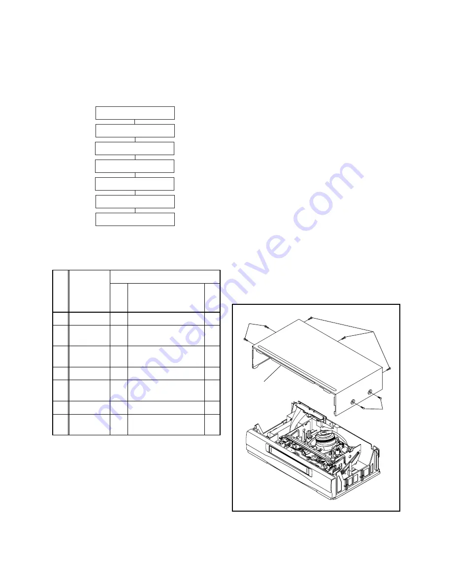
CABINET DISASSEMBLY INSTRUCTIONS

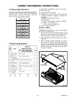
1. Disassembly Flowchart

This flowchart indicates the disassembly steps to gain
access to item(s) to be serviced.  When reassembling,
follow the steps in reverse order. Bend, route, and
dress the cables as they were originally.

2. Disassembly Method

(1): Identification (location) No. of parts in the figures

(2): Name of the part

(3): Figure Number for reference

(4): Identification of parts to be removed, unhooked,

unlocked, released, unplugged, unclamped, or
desoldered.
P=Spring, L=Locking Tab, S=Screw,
CN=Connector
*=Unhook, Unlock, Release, Unplug, or Desolder
e.g. 2(S-2) = two Screws (S-2),
       2(L-2) = two Locking Tabs (L-2)

(5): Refer to “Reference Notes.”

Reference Notes

CAUTION: Locking Tabs (L-1) and (L-2) are fragile.
Be careful not to break them.
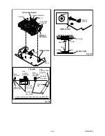
1. Remove five Screws (S-2), three Screws (S-3) and

Screw (S-4). Then, slowly lift the VCR Chassis Unit
(Deck Assembly, Jack CBA and Main CBA) up.

2. When reassembling, solder wire jumpers as shown

in Fig. D5.

3. Before installing the Deck Assembly, be sure to

place the pin of LD-SW on Main CBA as shown in
Fig. D6. Then, install the Deck Assembly while
aligning the hole of Cam Gear with the pin of LD-
SW, the shaft of Cam Gear with the hole of LD-SW
as shown in Fig. D6.

ID/

LOC

.No.

PART

REMOVAL

Fig. 

No.

REMOVE/*UNHOOK/
UNLOCK/RELEASE/
UNPLUG/DESOLDER

Note

[1]

Top Case

D1

7(S-1)

-

[2]

Front 
Assembly

D2

*3(L-1),*4(L-2)

-

[3]

VCR Chassis 
Unit

D3

5(S-2), 2(S-3), (S-4)

1

[4]

Jack CBA

D4

Desolder, (S-5)

-

[5]

Deck 
Assembly

D5
D6

(S-6A),(S-6B), Desolder

2,3

[6]

Main CBA

D5

----------

-

[7]

Cylinder 
Shield

D5

(S-7)

-

(1)

(2)

(3)

(4)

(5)

[5] Deck Assembly

[4] Jack CBA

[1] Top Case

[2] Front Assembly

[3] VCR Chassis Unit

[6] Main CBA

[7] Cylinder Shield

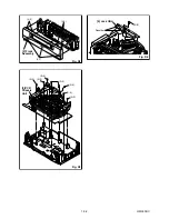
Fig. D1

(S-1)

(S-1)

(S-1)

[1] Top  Case

Содержание VC4006F

Страница 1: ...paration for Servicing I Adjustment Procedures I Schematic Diagrams I CBA s I Exploded views I Parts List When servicing the deck mechanism refer to MK14 Deck Mechanism Section Deck Mechanism Part No...

Страница 2: ...How to Initialize the VCR 1 7 1 Function Indicator Symbols 1 8 1 Block Diagrams 1 9 1 Schematic Diagrams CBA s and Test Points 1 10 1 Waveforms 1 11 1 Wiring Diagrams 1 12 1 IC Pin Function Descripti...

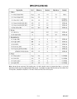
Страница 3: ...Vp p 0 8 1 0 1 2 1 3 Video S N Y R P dB 40 45 SP Mode W O Burst 1 4 Video Color S N AM R P dB 37 41 SP Mode 1 5 Video Color S N PM R P dB 30 36 SP Mode 1 6 Resolution PB Line 230 245 SP Mode 2 Servo 2...

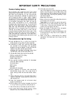
Страница 4: ...especially 1 Wires covered with PVC tubing 2 Double insulated wires 3 High voltage leads D Use specified insulating materials for hazardous live parts Note especially 1 Insulation tape 2 PVC tubing 3...

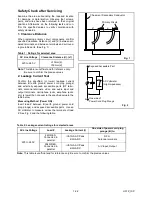
Страница 5: ...ts RF termi nals antenna terminals video and audio input and output terminals microphone jacks earphone jacks etc is lower than or equal to the specified value in the table below Measuring Method Powe...

Страница 6: ...flat pack IC with tweezers while applying the hot air 3 Bottom of the flat pack IC is fixed with glue to the CBA when removing entire flat pack IC first apply soldering iron to center of the flat pac...

Страница 7: ...by one using a sharp pin or wire to which solder will not adhere iron wire When heating the pins use a fine tip soldering iron or a hot air desoldering machine Fig S 1 4 3 Bottom of the flat pack IC i...

Страница 8: ...s Fig S 1 6 Note When using a soldering iron care must be taken to ensure that the flat pack IC is not being held by glue When the flat pack IC is removed from the CBA handle it gently because it may...

Страница 9: ...ed to remove any static electricity that may be charged on the body 2 Ground for Workbench Be sure to place a conductive sheet or copper plate with proper grounding 1 M on the workbench or other surfa...

Страница 10: ...nto the Deck Mechanism Assembly and press the PLAY button The tape will be loaded into the Deck Mechanism Assembly Make sure the power is on connect TP507 S INH to GND This will stop the function of T...

Страница 11: ...ragile Be careful not to break them 1 Remove five Screws S 2 three Screws S 3 and Screw S 4 Then slowly lift the VCR Chassis Unit Deck Assembly Jack CBA and Main CBA up 2 When reassembling solder wire...

Страница 12: ...1 5 2 HM340DC Fig D2 L 2 L 1 2 Front Assembly L 2 Fig D3 S 2 S 2 S 4 S 2 S 2 S 3 S 3 3 VCR Chassis Unit Fig D4 S 5 4 Jack CBA Desolder...

Страница 13: ...om Cylinder Assembly From ACE Head Assembly Lead with white stripe Lead with blue stripe Desolder from bottom Lead with blue stripe From Capstan Motor Assembly Lead connections of Deck Assembly and Ma...

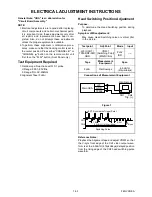
Страница 14: ...cope Dual trace with 10 1 probe V Range 0 001 50V Div F Range DC AC 20MHz 2 Alignment Tape FL6A Head Switching Position Adjustment Purpose To determine the Head Switching position during playback Symp...

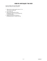
Страница 15: ...R as the following procedure 1 Make sure that no timer programming is set If not reset all timer programming 2 Turn the power off 3 Press the STOP EJECT button and CHANNEL K button on the unit simulta...

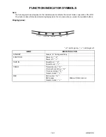
Страница 16: ...d on the tv screen when you press the operation buttons Display panel H LED Light on L LED Light off MODE INDICATOR ACTIVE STANDBY Always H during electricity FUNCTION Power on H Power off L TAPE IN C...

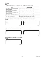
Страница 17: ...tion Cause Indicator Active When reel or capstan mechanism is not functioning correctly A R is displayed on a TV screen Refer to Fig 1 When tape loading mechanism is not functioning correctly A T is d...

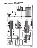
Страница 18: ...TO AUDIO BLOCK SDA SDA SCL SCL TU701 TUNER UNIT IC503 MEMORY 72 83 IIC BUS SCL D V SYNC D REC H RF SW H A SW C ROTA IIC BUS SDA H A COMP V ENV C SYNC TRICK H SECAM H IIC BUS SCL 71 3 5 SDA SCL 12 11...

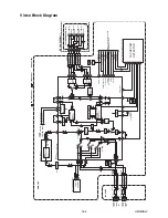
Страница 19: ...501 OSD REC VIDEO SIGNAL PB VIDEO SIGNAL MODE SP REC SERIAL DECORDER VIDEO OUT1 1 VIDEO IN1 1 3 3 VIDEO OUT2 1 VIDEO IN2 3 1 3 JACK CBA IC370 PAL SECAM DECTECTOR PAL SECAM DETECTOR 48 50 52 56 24 6 50...

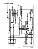
Страница 20: ...H 5 AE H FE H AUDIO HEAD AUDIO ERASE HEAD ACE HEAD ASSEMBLY FE HEAD 2 FE H 1 FE H GND CN501 MAIN CBA PB AUDIO SIGNAL REC AUDIO SIGNAL Mode SP REC 71 A MUTE H AUDIO SW 1 AUDIO SW 2 IIC BUS SCL IIC BUS...

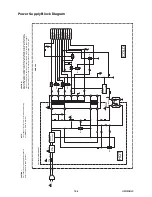
Страница 21: ...18 T1 6A L 250V Q055 Q059 SHUNT REGULATOR CAUTION Fixed voltage or Auto voltage selectable power supply circuit is used in this unit If Main Fuse F001 is blown check to see that all components in the...

Страница 22: ...itute replacement parts that do not have the same safety characteristics as specified in the parts list may create shock fire or other hazards Notes 1 Do not use the part number shown on these draw in...

Страница 23: ...n original function and reliability of repaired units use only original replacement parts which are listed with their part numbers in the parts list section of the service manual 4 Mode SP REC 5 Volta...

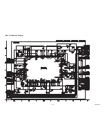
Страница 24: ...1 10 3 HM320SCM1 Main 1 6 Schematic Diagram...

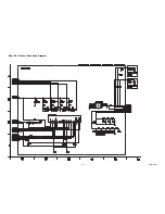
Страница 25: ...1 10 4 HM320SCM2 Main 2 6 Sensor Schematic Diagram...

Страница 26: ...1 10 5 HM320SCM3 Main 3 6 Schematic Diagram...

Страница 27: ...1 10 6 HM320SCM4 Main 4 6 Jack Schematic Diagram...

Страница 28: ...fire hazard replace only with the same type fuse CAUTION Fixed voltage or Auto voltage selectable power supply circuit is used in this unit If Main Fuse F001 is blown check to see that all components...

Страница 29: ...1 10 8 HM320SCM6 Main 6 6 Schematic Diagram...

Страница 30: ...is used in this unit If Main Fuse F001 is blown check to see that all components in the power supply circuit are not defective before you connect the AC plug to the AC power supply Otherwise it may c...

Страница 31: ...s unit If Main Fuse F001 is blown check to see that all components in the power supply circuit are not defective before you connect the AC plug to the AC power supply Otherwise it may cause some compo...

Страница 32: ...1 10 11 BHM450F01011C Jack CBA Top View Jack CBA Bottom View...

Страница 33: ...LOR BAR SIGNAL WITH 1KHz AUDIO SIGNAL WF1 WF3 WF3 V OUT E E 10 s 50mV x 10 J23 WF3 UPPER WF1 LOWER V OUT 0 1V x 10 RF SW 0 5V x 10 50 s J23 TP502 WF2 C PB 10mV x 10 RF SW 0 5V x 10 5ms UPPER LOWER WF1...

Страница 34: ...FE H GND 1 CN501 CN502 CN504 CN253 GND 1 VIDEO OUT1 2 AL 12V 1 3 VIDEO IN1 4 AUDIO R OUT1 5 JK1 8P OUT 6 AUDIO L IN1 7 1 2 3 4 5 6 7 CN151 CN101 FULL ERASE HEAD FE HEAD VIDEO R 1 HEAD VIDEO L 1 HEAD...

Страница 35: ...RF SW Video Head Switching Pulse H L 19 NU Not Used 20 NU Not Used 21 NU Not Used 22 NU Not Used 23 OUT POWER LED STANDBY LED Sig nal Output H 24 OUT CAS LED TAPE IN LED Signal Output H 25 OUT TIMER L...

Страница 36: ...Control Signal PWM 77 OUT D CONT Drum Motor Control Signal PWM 78 OUT C F R Capstan Motor FWD REV Control Signal FWD L REV H H L 79 IN S REEL Supply Reel Rotation Signal PULSE Pin No IN OUT Signal Na...

Страница 37: ...A103M AT P KRC103M AT P KTA 1266 GR AT P KTA1267 GR Y AT P KTC3199 BL GR Y AT P RN2204 TE4 F T 2SA1015 GR TE2 F T 2SC1815 BL GR Y TE2 F T 2SC2120 Y TE2 F T KTA1281Y AT P KTC3203 Y AT P BR24L02F WE2 CA...

Страница 38: ...1 15 1 HM320FEX EXPLODED VIEWS Front Panel A1X...

Страница 39: ...r parts with this mark Some Ref Numbers are not in sequence 2B18 A2 2L011 2L011 2L011 2L011 2L011 2B9 2B9 2L022 2L022 2L012 JACK CBA A5 2L041 A10 2L031 2L099 2L041 2B7 SENSOR CBA 2B8 2B46 A7 A3 2L042...

Страница 40: ...1 15 3 HM320PEX Packing Some Ref Numbers are not in sequence X3 X20 X1 X4 S1 Unit S3 A14 S2 S2 X2 X6 S7...

Страница 41: ...CUSHION HC460ED 0VM413251 2B18 FIBER TOP CASE HC460ED 0VM412906 2L011 SCREW P TIGHT 3X10 BIND HEAD GBCP3100 2L012 SCREW P TIGHT 3X10 BIND HEAD GBCP3100 2L021 SCREW P TIGHT M3 10 WASHERHEAD GCJP3100 2L...

Страница 42: ...MIC CAP 1608 CH J 470pF 50V CHD1JJ3CH471 C151 CHIP CERAMIC CAP 1608 F Z 0 1 F 50V or CHD1JZ30F104 CHIP CERAMIC CAP 1608 F Z 0 1 F 25V CHD1EZ30F104 C152 CHIP CERAMIC CAP 1608 F Z 0 1 F 50V or CHD1JZ30F...

Страница 43: ...AP B K 2200pF 50V CHD1JK30B222 C383 CHIP CERAMIC CAP B K 2200pF 50V CHD1JK30B222 C384 ELECTROLYTIC CAP 2 2 F 50V M H7 or CE1JMAVSL2R2 Ref No Description Part No ALUMINUM ELECTROLYTIC CAP 2 2 F 50V H7...

Страница 44: ...4148M SWITCHING DIODE 1SS133 T 77 QDTZ001SS133 D008 SWITCHING DIODE 1N4148M or NDTZ01N4148M SWITCHING DIODE 1SS133 T 77 QDTZ001SS133 D009 SWITCHING DIODE 1N4148M or NDTZ01N4148M SWITCHING DIODE 1SS133...

Страница 45: ...9P TRANSISTOR KTC3199 GR AT P or NQS4KTC3199P TRANSISTOR 2SC1815 Y TE2 F T or QQSY2SC1815F TRANSISTOR 2SC1815 GR TE2 F T QQS12SC1815F Ref No Description Part No Q563 TRANSISTOR KTC3199 Y AT P or NQSYK...

Страница 46: ...RRXAJR5Z0103 RES CHIP 1608 1 10W J 10k RRXA103YF002 R320 CHIP RES 1 10W J 1k or RRXAJR5Z0102 Ref No Description Part No RES CHIP 1608 1 10W J 1 0k RRXA102YF002 R321 CARBON RES 1 6W J 33 or RCX6JATZ033...

Страница 47: ...33k RRXA333YF002 R534 CARBON RES 1 6W G 3 6k or RCX6GATZ0362 CARBON RES 1 4W G 3 6k RCX4GATZ0362 Ref No Description Part No R535 CARBON RES 1 6W G 10k or RCX6GATZ0103 CARBON RES 1 4W G 10k RCX4GATZ01...

Страница 48: ...04 PB F VRCB104HH014 X301 XTAL 4 433619MHz or FXC445LLN004 XTAL 1K 044334EE or FXC445LDS002 QUARTZ CRYSTAL 4 433619MHz FXC445LCHE01 Ref No Description Part No X501 XTAL 12MHz 12 000MHz or FXD126LDS002...

Страница 49: ...1 10W J 220 RRXA221YF002 R127 CHIP RES 1608 1 10W 0 or RRXAZR5Z0000 RES CHIP 1608 1 10W J 0 RRXA000YF002 MISCELLANEOUS 2L022 SCREW P TIGHT M3 10 WASHERHEAD GCJP3100 A5 JACK BOARD 2 21P HE470ED 0VM203...

Страница 50: ...VC4006F HM320FD 2006 05 24...

Отзывы: