INT
J2
1
2
3
4
6
5
7
8
R103
10K
C30
105
K2
K3
R74
10K
R75
10K
VCC
K4
SCL
XRES
VDL
GND
SDA
U15
CY8C21534
P07
1
P05
2
P03
3
P01
4
P27
5
P25
6
P23
7
P21
8
VSS
9
P17
10
P15
11
P13
12
SCL
13
VSS
14
VDD
28
P06
27
P04
26
P02
25
P00
24
P26
23
P24
22
P22
21
P20
20
XRES
19
P16
18
P14
17
P12
16
SDA
15
VDL
VLED
D_GND
PSOC_SDA
PSOC_SCL
R4
100R
R9
100R
K6
K4
K2
K5
K3
K1
K1
K5
K6
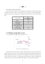
Figure 3.2.8.1Button circuit diagram
3.2.7 Headphone output jack circuit
1. Headphone output jack circuit principle diagram is shown in the picture 3.2.7.1:
2. Working principle: left/right channel audio signals that output from Wm8750 output through
220uF capacitor coupling. D1 in the circuit is TVS diode array used for ESD protection. Ground wire of
headphone is also used as antenna input of FM module.
3.2.8 Button circuit
1. Button circuit diagram is shown in the picture 3.2.8.1:
Figure 3.2.7.1 Headphone output jack circuit
OUT_L1
L3
601/0603
D1
RCLAMP0504F/SC-70
1
6
2
3
4
5
L1
601/0603
L5
601/0603
R99
1K
CN1
2SJ-A382-001(HP-DC)
1
4
3
5
OUT_R1
R100
1K
GND
FM_ANT
C32 220UF/4V
C31 220UF/4V
R102
0R*
HP_OUTL
C90
104
R83
10R
C92
104
R84
10R
HP_OUTR
2. Working principle: V3/V5 adopts touch button and button control IC is CY8C21434. CY8C21434
integrates the programmable digital and analog system inside, which may configure various functional
modules needed by users flexibly, and it is a really system (SoC) with mixed signals processing ability.
CY8C21434 chip belongs to capacitor touch mode, which adopts I2C bus control.
- 23 -
Содержание V3N
Страница 1: ...service manual V3N V3H V5N V5H ...
Страница 66: ...Chapter Cinque PCB board Circuit diagram Section One PCB board 5 1 1 Surface layer of Main Board 61 ...
Страница 67: ...5 1 2 Bottom layer of Main Board 62 ...
Страница 79: ...Chapter Eight V5 PCB board Circuit diagram Section One PCB board 8 1 1 Surface layer of Main Board 74 ...
Страница 80: ...8 1 2 Bottom layer of Main Board 75 ...

