background image

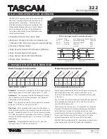
Principle of compressing the acoustic signat’s dynamic 

range.

  whisper etc. have merely disappeared. To 

avoid this, you just have to decrease the volume 
of “loud” sounds by simultaneously increasing 
the volume of “soft” sounds with the volume of 
“average” sounds left unchanged, i.e. Just 
decrease the dynamic range of sound 
accompaniment. Only Dolby Digital system 
provides for such a method of sound control. It 
uses the principle of compressing the acoustic 
signal’s dynamic range while recording; 
therefore, while playing an inverse 
transformation(volume expansion) takes place. 
This is called”night” mode. The regulation limits 
are restricted, however, to avoid distortions of 
resultant signal.

The Dolby Digital system provides an 

extremely broad dynamic range of playback 
sound-from gentle to roaring. It creates the 
presence effect, especially while seeing motion 
pictures. However, at night a powerful sound 
with a broad dynamic range may give pleasure 
to you ,but disturb and annoy your family and 
neighbors. If you just decrease the volume, you 
will immediately notice that you ceased  to hear, 
e, g, dialogues  as clear as you do at normal 
volume, and such sound effects as rustle,

“Night” mode

Fig.1.Delay of central 
channel=0

Fig.2.Small area Delay 
of central channel=L=(or 

Fig.3.Small area Delay 
of central channel=0
        L=R>C

Dolby Digital

Dolby Pro Logic s urround

Rear channel

Stereo 20 Hz -20 kHz

Mono channel with li mited frequency
range(100Hz-7 kHz )

Low-frequency
channel(s ubwoofer)

Available,20-120 Hz

N/a

Sound field dis tribut ion

Muitivariate

From left t o right,  from right to left, from
front to rear, from rear t o front

Channels

6 independent c hannels,  each
reproducing it s own si gnal at a t ime

4 segment ed channels . Only  one channel
is dec oded at a ti me.

Creates an opt imum s ound field with
illus ion of an equal distance from listener
to each speaker.

The most c ost-efficient way  to ensure
high-qualit y surround effect.

Allows  adjust ing the dec ompress ion
degree of sound infromati on("night "
mode).

Surround sound m ay be received from
any signal source.

Miscellaneous

- 12 -

Содержание DV118SI

Страница 1: ...service manual VerSI09 16 A DV 18SI RU DV118SI 1 ...

Страница 2: ... 3 Required device for maintenance Chapter Two Functions and Operation Instructions 2 1Features 2 2 2 2 1 2 2 2 2 2 3 2 2 4 2 3 2 4 2 4 1 2 4 2 2 4 3 2 4 4 2 4 5 Chapter One About Maintenance Controls and functions Front and side panels control Rear Panel general view LED display general view NO DISPLAY FOR DV118SI Remote Control general view Set list FUNCTION SETTINGS Function selection and chang...

Страница 3: ...shooting 2 5 3Specification 4 2 Decode Circuit 4 3 Video Circuit 4 4 Audio Circuit 4 5 Power Circuit Chapter Five Troubleshooting Flow Chart Chapter Six Waveform Diagram Chapter Seven PCB board 7 1 Surface layer of Decode Board SKY_CX2 03 2009 07 20 7 2 Surface layer of AV Board NO SCART OUTPUT2006 12 25 FOR DV118SI 7 3 Bottom layer of AV Board 7 4 Power Board SKY V22 CX2 2009 11 18 Ver2 0 7 5 Sur...

Страница 4: ...Chapter Eight 8 1 Decode Board SKY_CX2 03 2009 07 20 8 2NO AV Board SCART OUT 2006 12 25 8 3 Power Board SKY V22 CX2 2009 11 18 8 4 Main Panel DV214 216SI PCB V2 0 8 5 OK Board DV214 216SI MIC PCB 8 6 USB Board DV214 216SI PCB V2 0 Chapter Nine BOM List Circuit Diagram 30 30 31 31 34 35 36 37 38 39 For DV118SI ...

Страница 5: ...Caution This service manual is only applicable to DV118SI RU SI09 16 A ...

Страница 6: ...h of about 2 metres to insert into the earth and Fetch the lead wire from the top of the surplus metal and connect to the required static electricity device The length and depth of the metal embedded under the earth should be determined according to the wettability of the local soil For humid places it may be shorter and longer and deeper for dry places If possible it can be distributed and layed ...

Страница 7: ...But in the circuit the tested numerical value of resistance is not accurate and the tested numerical value of integrated IC s pins can only be used for reference so the elements should be broken down for test 1 2 3 Voltage method Voltage method is relatively convenient quick and accurate Set the multimeter in voltage position and test power supply voltage of the player and voltage of a certain poi...

Страница 8: ... with those tested through fault PC board the cause of troubles may be found Through the above maintenance method theoretical knowledge and maintenance experience all difficulties and troubles will be readily solved 1 3 Required device for maintenance Digital oscillograph 100MHE TV set SMD rework station Multimeter Soldering iron Pointed month pincers Cutting nippers Forceps Electric screw driver ...

Страница 9: ...n Output Y Pb Pr producing flicker free and stable images Composite component Y Cb Cr S Vidio and RGB SCART outputs for various types of Connections Capable of playing NTSC PAL discs written in NTSC system Multiple dubbings angles subtitles support Sharpness gamma brightness contrast hue saturation adjustment Others Compatible disc types CD R CD RW DVD R DVD RW DVD R DVD RW USB interface to connec...

Страница 10: ...yback PLAY PAUSE button Press to playback pause Disc tray USB port Phones jack 5 6 7 8 9 10 11 NOTE Presence and location of the buttons sockets and regulators depend on a model of DVD player 2 9 2 2 2 Rear Panel general view Stereophonic audio output Socket of video output S Video Socket of composite video output 1 2 3 4 5 Socket of coaxial digital audio output NOTE Presence and location of the b...

Страница 11: ...layback from the previous point REPEAT button Press to repeat playback A B buttons Press to repeat the selected portion Button Press to turn on off the sound VOLUME button Press to adjust the volume DVD USB button Press to switch DVD USB models Button Press to playback from the following point Button Press to stop playback Button Press to forward scanning Button Press to play pause the playback ZO...

Страница 12: ...an Default option English High Medium Low TV system TV scan mode Video output TV format Sharpness Gamma Brightness Contrast Hue Saturation AUTO IS S Vid 4 3 LB Med Off 48 48 0 0 DVD player Audio cord Video cord Remote control Battery AAA Warranty card User s manual 1PCS 1PCS 1PCS 1PCS 2PCS 1PCS 1PCS 2 3 Set list TV system TV scan mode Video output TV format Sharpness Gamma Brightness Contrast Hue ...

Страница 13: ...ge contrast 9 Hues adjustment of image hues 10 adjustment of image saturation Adjustment of image brightness contrast hues and saturation Select the desired item of the image adjustment section using the Up and Down buttons Press OK or RIGHT key to start adjusting the relevant option Change the option value using the Up and Down buttons Upon completion press the LEFT key of the UP and DOWN buttons...

Страница 14: ...6 bit 3 Sound correction A Max volume max volume limiting Using the Up and Down buttons adjust the max volume level Press the LEFT key of the Up and Down buttons to return to sound correction setup menu B Equalizer equalizer modes Options Rock Pop Live Dance Techno Classic Soft Default option Off C Echo echo effects Options Off Concert Living room Hall Bathroom Cave Arena Church Default option Off...

Страница 15: ...ons Press LEFT key of the UP DOWN buttons to return to karaoke settings menu 2 4 7 Preference settings 1 Gr Equalizer spectrum analyzer Options On Off Default option Off 3 Screensaver screen saver on off Options On off Default option On 10 On Off Gr Equalizer Screensaver Off On 2 4 8 Parental Control 1 Category setup of age restrictions to prevent children from seeing undesirable discs Options Any...

Страница 16: ... front speakers inches Fig 3 Detemine delay value as to Dolby Digital mode Set up of time delay in the central channel Sometimes several people are listening to the music and the space is limited In this case you can install three speakers two front ones and a central one as shown in Fig 1 with the distance to the listener being approximately the same The central channel delay is to be set at 0 Sh...

Страница 17: ...may give pleasure to you but disturb and annoy your family and neighbors If you just decrease the volume you will immediately notice that you ceased to hear e g dialogues as clear as you do at normal volume and such sound effects as rustle Night mode Fig 1 Delay of central channel 0 Fig 2 Small area Delay of central channel L or Fig 3 Small area Delay of central channel 0 L R C Dolby Digital Dolby...

Страница 18: ...f malfunction before addressing the service center Sign of trouble Cause of trouble Actions to eliminate the trouble No sound 1 Poor audio cable connection 2 Disc dirty or damaged 3 Sound disabled by the MUTE button 1 Make proper connection 2 Clean the disc 3 Press the MUTE button No image 1 Poor video cable connection 2 Incorrect settings of your TV set 3 The DVD player is in the progressive scan...

Страница 19: ...utput RGB SCART output Composite output Audio characteristics Voltage range Temperature requirement Moisture requirement 15 75 not condensate Outputs C 0 286Vp p 75 Signal swing of component video output 1 0Vp p 75 Signal swing of composite video output 1 0Vp p 75 Signal swing of S Video output 1 0Vp p 75 DVD Video Super VCD VCD MPEG 4 CD DA CD G HDCD MP3 WMA Kodak Picture CD JPEG CD R CD RW DVD R...

Страница 20: ... F GND V20 VCC E VR CD VR DVD LD CD MDI HFM VCC LD DVD GND RGB_CVBS R V G Y GND B U AV_TV VIDEO L AGND R DECODE BOARD SKY_CX2 03 2009 07 20 MIC1 MIC2 GND FS0 LEDAT LEDCK LEDST GND VCC IR 12 V 12 V GND 5V GND VCC POWER BOARD SKY V22 CX2 MAIN PANEL OK BOARD DV214 216SI MIC PCB CN6 CN3 CN5 CON7 CN602 FS0 VSDA VSCK VSTB GND VCC IR KEY KEY CN4 VCC USB_DM USB_DP GND CON3 VCC USB_DM USB_DP GND AV BOARD S...

Страница 21: ...LD_DVD LD_CD CD DVD Switch Laser power control MDI DVD A B C D RFO CD A B C D E F V20 TRIN TROUT LIMIT MT1389L LOADER U2 AM5888 T T F F SL SL SP SP LOAD LOAD M M M Feed Motor Spindle Motor Door open close circuit Audio Amplify Filter U6 U7 U8 AL AR ALS ARS ARF ALF ASPDIF FL FR SL SR LFE CC U1 V_B V_R V_G CVBS SY_B U SC_R V CVBS G Y1 B PB R PR Video Filter Clamping MIC board MIC1 U9 FLASH Ou t p u ...

Страница 22: ...sing chip MT1389 and driving chip AM5888 MT1389 is also main part of decode circuit Block diagram of servo circuit is shown in figure 4 1 1 FOSO FMSO TRSO DMSO A B C D E F RFO IOA LDO2 LDO2 MDI1 Disc switch circuit Laser power control circuit Spindle control detecting circuit Spindle Motor Feed Motor XS1 AM5888 MT1389L Door open close circuit T T F F SL SL SP SP 1 23 4 26 15 16 14 13 17 18 12 11 F...

Страница 23: ...video output has R B G Y Pb Pr Y Cb Cr CVBS and Y C output modes in which R B G Y Pb Pr Y Cb Cr and Y C can not output at the same time and need to be switched via software CVBS is a separate output mode four channel video signal is outputted to AV board by MT1389 after video filtering and clamping Block diagram of video signal process is shown in figure 4 Figure 4 3 1 Block diagram of video signa...

Страница 24: ...T XS7 AL AR ALS ARS ALF ARF OKA 92 4558 U6 4558 U7 4558 U8 C71 C81 C79 C77 C75 C73 AL AR ALS ARS ALF ARF XS8 R68 IEC958 4 5 Power Circuit 1 Block diagram of power circuit is shown in figure 4 5 1 Figure 4 5 1 Block diagram of power circuit Transformer Rectify Absorb loop Electric net filter Insurance tube Power socket Switch IC Feedback winding Opto coupler LM 431A Sample circuit Rectify Filter 10...

Страница 25: ...ck whether it is on A1 Check whether power board outputs voltage normally Check power supply circuit of decode board Check whether panel power supply is normal Check whether working voltage of indication light is normal whether indication light is damaged Check whether power board U501 U502 and U503 are normal working Check whether power supply of FLASH is normal Check whether clock is normal Chec...

Страница 26: ... Check whether L3 inductance is high level Replace loader pick up Check whether power supply Q4 is normal Replace MT1389 chip Check multilink power supply of Q4 triode Check whether DVD disc is readable Refer to troubleshooting flow chart of unreadable CD disc Check whether composite video output is normal Unplug XS7 XS8 flat cable of decode board to check whether video output is normal Check whet...

Страница 27: ...e has sound output Replace MT1389 chip Replace 4558 chip Check whether karaoke is normal Whether software is open Check whether MIC board karaoke signal is normal Replace MT1389 chip Turn on MIC switch ON Check whether power supply of 4558 is normal Check power supply circuit Check whether pin 7 has karaoke signal output Replace microphone socket Replace 4558 chip Troubleshooting of player is fini...

Страница 28: ...rpose to help servicing personnel to judge where trouble lies in accurately and quickly to improve servicing skills For the difference of oscillograph s type model and tuner a certain difference may exist so the servicing personnel are expected to pay more attention to check in daily operation 2 Waveform diagram for spindle signal DMO when spindle has motion Vpp 28 0V Vpp 12 1V 23 ...

Страница 29: ...r feed signal FMO when pick up has feed motion 4 Waveform diagram for traction signal TRO when pick up has traction motion 5 Waveform diagram for focus signal FOO when pick up has focus motion Vpp 13 4V Vpp 4 2V Vpp 5 1V 24 ...

Страница 30: ...6 Waveform diagram for FLASH chip SF_DI pin 5 of U5 7 Waveform diagram for FLASH chip SF_CK pin 6 of U5 8 Waveform diagram for 27MHz clock X1 Vpp 4 08V Vpp 3 40V Vpp 1 12V 25 ...

Страница 31: ... waveform diagram 10 Video signal waveform diagram 11 1KHZ audio signaal output waveform diagram it is suggested to use test disc if not waveform tested will change at any time which will affect your judgment Vpp 4 60V 26 ...

Страница 32: ...Chapter Seven PCB Board 7 1 Surface layer of Decode Board SKY_CX2 03 2009 07 20 27 ...

Страница 33: ...e layer of AV Board DV214 216SI NO AV Board For DV118SI 7 3 Bottom layer of AV Board DV214 216SI 7 4 Power Board SKY V22 CX2 28 NO AV Board For DV118SI Surface layer of Bottom layer of 7 5 Power Board SKY V22 CX2 ...

Страница 34: ...7 5 Surface layer of Main Panel DV214 216SI PCB V2 0 7 7 USB Board 29 7 6 Bottom layer of Main Panel DV214 216SI PCB V2 0 DV214 216SI PCB V2 0 ...

Страница 35: ...7 8 Surface layer of OK Board DV214SI DV216SI DV118SI MIC PCB V2 0 7 9 Bottom layer of OK Board 30 DV214SI DV216SI DV118SI MIC PCB V2 0 ...

Страница 36: ...7 10k Q5 2SB1132 1 3 2 C72 0 015uF D11 BAT54C 1 3 2 L8 150uH C63 0 1uF R11 1 C25 0 1uF D3 IN5401 1 2 R24 10 C35 6800pF C37 0 1uF R16 560 R27 0 C164 0 1uF R20 0 TOP CN5 SMD24P0 5mm 1 2 3 4 5 6 7 8 9 10 11 12 13 14 15 16 17 18 19 20 21 22 23 24 R9 1k R39 10k R41 10k C69 330pF R18 100k C59 0 1uF L11 47uH Q4 2SB1132 1 3 2 C163 0 1uF D2 IN5401 1 2 C43 4 7uF R3 10 C47 10uF 10v R49 10k Q1 2N3904 1 3 2 C6...

Страница 37: ...O ASPECT G Y_OUT R V_OUT CENT SUB LSCH RSCH CN13 7P 2mm 1 2 3 4 5 6 7 CN10 7P 2mm 1 2 3 4 5 6 7 COAXIAL G Y_OUT B U_OUT RCH LCH R V_OUT P3 RCA2X3JACK 1 4 6 8 5 7 9 2 3 V_B B U_OUT SC VCC VCC R144 0 R145 NC R68 75 1 C108 100pF C109 100pF D15 BAV99 SMD 1 3 2 Q24 NC 1 3 2 L26 1 8uH CVBSO Y S C S G G C Y P2 YC_JACK 3 4 2 1 7 8 9 5 6 V_G G Y_OUT VCC VCC R147 NC R146 0 Q25 NC 1 3 2 L27 1 8uH R78 75 1 D1...

Страница 38: ...3906 1 3 2 D10 1N4148 R82 100k C118 220uF 10v C155 100uF 16v R85 10k C119 47uF 16v R87 47k D8 1N4148 R86 NC D7 1N4148 AL 12V 12V A_MUTE LCH C124 10uF 16v C126 1000pF R97 100k R96 100k R91 10k R92 5 1k C125 1000pF C122 100pF Q13 2N3904 1 3 2 R89 31k U11A NJM4558 3 2 1 8 4 C123 10uF 16v R95 470 12V 12V 12V 12V C95 0 1u C96 0 1u C97 0 1u C99 0 1u C100 0 1u C101 0 1u ASPECT FS1 FS0 12V Q14 2N3904 1 3 ...

Страница 39: ...1 32 33 34 35 36 37 38 39 40 41 42 43 44 45 46 47 48 49 50 VCC DQ0 DQ1 VSSQ DQ2 DQ3 VCCQ DQ4 DQ5 VSSQ DQ6 DQ7 VCCQ DQML WE CAS RAS CS BA A11 A10 A0 A1 A2 A3 VCC VSS A4 A5 A6 A7 A8 A9 NC CKE CLK DQMH NC VCCQ DQ8 DQ9 VSSQ DQ10 DQ11 VCCQ DQ12 DQ13 VSSQ DQ14 DQ15 VSS R51 10k U5 ESMT M12L64164A N C 1 2 4 12 5 7 9 8 10 46 11 13 15 16 17 18 19 35 22 23 24 25 26 14 41 29 30 31 32 33 34 36 37 38 39 40 43 4...

Страница 40: ... 220K 1 2W R512 9 1K U502 HS817 TC502 47uF 50V TC501 10uF 400V TC504 220uF 25V TC506 470uF 16V TC505 1500uF 16V TC503 220uF 25V D505 FR107 D508 FR107 D510 IN5822 D506 FR107 D511 D503 1N4007 D502 1N4007 D504 1N4007 D501 1N4007 4 VDD 5 D 2 S 3 FB 6 D 7 D 8 D 1 S U501 VIPER22 1 _ 3 _ 4 _ 5 _ 6 _ 7 __ 8 _ 9 _ T501 EEL19H 1 2 CON1 220V 5V 12V 12V CX2 R509 0805 9 1K改为0805 10K TC500 4 7uF 400V L502 1mH 1...

Страница 41: ...ain Panel DV214 216SI PCB V2 0 36 1 2 3 U1 ARM3837B1 L SW3 SW1 SW2 C1 104 R1 100 IR VCC EC1 100uF 16V DST DCK DAT VCC GND IR 2 3 4 1 5 6 CN1 DST DCK DAT 1 K 2 D1 IN4148 R6 4 7K R2 4 7K R4 4 7K VCC 7 I O SW4 ...

Страница 42: ... 4940956 37 MIC MIC2 MIC1 DV33 12V C165 1u C167 100p R157 1k R154 0 R153 NC D9 1N4148 R156 1k R155 1k R158 1 2K Q26 2N3904 1 3 2 C166 100p R159 33k C168 1u AKIN1 MIC MIC1 MIC2 C138 0 1uF R112 100 CN11 3P 2mm 1 2 3 C142 3300pF ...

Страница 43: ... 38 8 6 USB Board DV214 216SI PCB V2 0SI 0 1 GND 2 D 3 D 4 VCC USB_JACK C902 104 TC901 10V100U L901 FBSMT 2 3 4 1 CN4 GND USBP USBM VCC USBM USBP VCC GND ...

Отзывы: