163
4317I–AVR–01/08
AT90PWM2/3/2B/3B
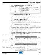
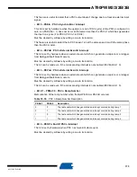
• Bit 3 – POEN2D : PSCOUT23 Output Enable (PSC2 only)
When this bit is clear, second I/O pin affected to PSCOUT23 acts as a standard port.
When this bit is set, second I/O pin affected to PSCOUT23 is connected to the PSC waveform
generator B output and is set and clear according to the PSC operation.
• Bit 2 – POENnB: PSC n OUT Part B Output Enable
When this bit is clear, I/O pin affected to PSCOUTn1 acts as a standard port.
When this bit is set, I/O pin affected to PSCOUTn1 is connected to the PSC waveform generator
B output and is set and clear according to the PSC operation.
• Bit 1 – POEN2C : PSCOUT22 Output Enable (PSC2 only)
When this bit is clear, second I/O pin affected to PSCOUT22 acts as a standard port.
When this bit is set, second I/O pin affected to PSCOUT22 is connected to the PSC waveform
generator A output and is set and clear according to the PSC operation.
• Bit 0 – POENnA: PSC n OUT Part A Output Enable
When this bit is clear, I/O pin affected to PSCOUTn0 acts as a standard port.
When this bit is set, I/O pin affected to PSCOUTn0 is connected to the PSC waveform generator
A output and is set and clear according to the PSC operation.
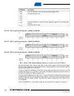
16.25.4
Output Compare SA Register – OCRnSAH and OCRnSAL
16.25.5
Output Compare RA Register – OCRnRAH and OCRnRAL
16.25.6
Output Compare SB Register – OCRnSBH and OCRnSBL
Table 16-12. Synchronization Source Description in Centered Mode
PSYNCn1
PSYNCn0
Description
0
0
Send signal on match with OCRnRA (during counting down of PSC). The
min value of OCRnRA must be 1.
0
1
Send signal on match with OCRnRA (during counting up of PSC). The
min value of OCRnRA must be 1.
1
0
no synchronization signal
1
1
no synchronization signal
Bit
7
6
5
4
3
2
1
0
–
–
–
–
OCRnSA[11:8]
OCRnSAH
OCRnSA[7:0]
OCRnSAL
Read/Write
W
W
W
W
W
W
W
W
Initial Value
0
0
0
0
0
0
0
0
Bit
7
6
5
4
3
2
1
0
–
–
–
–
OCRnRA[11:8]
OCRnRAH
OCRnRA[7:0]
OCRnRAL
Read/Write
W
W
W
W
W
W
W
W
Initial Value
0
0
0
0
0
0
0
0
Bit
7
6
5
4
3
2
1
0
–
–
–
–
OCRnSB[11:8]
OCRnSBH
OCRnSB[7:0]
OCRnSBL
Содержание AT90PWM2
Страница 344: ...346 4317I AVR 01 08 AT90PWM2 3 2B 3B 31 1 SO24...
Страница 345: ...347 4317I AVR 01 08 AT90PWM2 3 2B 3B 31 2 SO32...
Страница 346: ...348 4317I AVR 01 08 AT90PWM2 3 2B 3B 31 3 QFN32...
Страница 347: ...349 4317I AVR 01 08 AT90PWM2 3 2B 3B...


