


2.7
Thin Links
Thin Links master and slave interfaces connect the Juno r2 SoC to the daughterboard through the
motherboard tile site.
This section contains the following subsections:
•
2.7.1 Overview of Thin Links master and slave interfaces
•
2.7.2 Thin Links master interface
•
2.7.3 Thin Links slave interface in non-coherent mode
•
2.7.4 Thin Links slave interface in coherent mode
2.7.1
Overview of Thin Links master and slave interfaces
The Juno r2 SoC contains one AXI master interface and one slave interface, that you can use in either
coherent or non-coherent mode, that connect to the FPGA in the LogicTile Express daughterboard fitted
in the V2M-Juno r2 motherboard tile site. A Thin Links TLX-400 interface compresses the master and
slave interfaces to reduce the pin count.
The width of the TLX-400 slave interface on the Juno r2 SoC is greater than the width of the master
interface.
The Thin Links ACE slave interface uses the same pins as the Thin Links AXI slave interface and
enables the connection of a cache-coherent component to the V2M-Juno r2 motherboard tile site. The
ACE slave interface is intended to be used in conjunction with the Thin Links AXI master interface.
When the Thin Links ACE slave interface is in use, one of the Juno r2 SoC clusters is disabled.
The default Thin Links clock frequency of 61.5MHz gives the following operating speeds:
• Juno r2 SoC master interface:
— Forward direction, that is, from the Juno r2 SoC to the FPGA: 68MBps.
— Reverse direction, that is, from the FPGA to the Juno r2 SoC: 78MBps.
• Juno r2 SoC slave interface:
— Forward direction, that is, from the FPGA to the Juno r2 SoC: 246MBps.
— Reverse direction, that is, from the Juno r2 SoC to the FPGA: 305MBps.
Note
ARM recommends that you operate the Thin Links interfaces at the default speeds. See
for an example
board.txt
configuration file that sets the Thin Links
clocks to 61.5MHz.
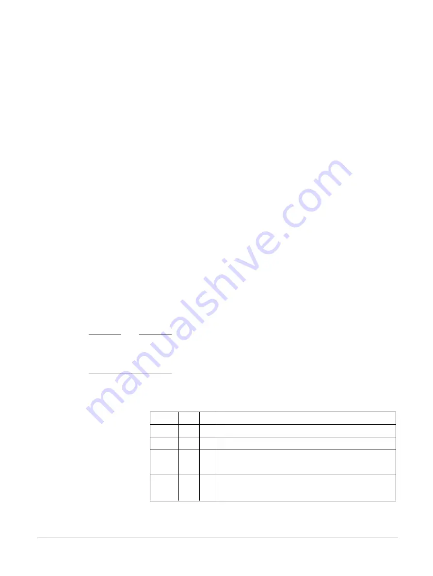
The following table shows the Thin Links timing requirements.
Table 2-3 Thin Links timing requirements
Symbol Min
Max Description
Tsu
1.2ns -
Input data parameter. Minimum data setup time before clock edge.
Th
1.0ns -
Input data parameter. Minimum data hold time after clock edge.
Tcomin
-2.5ns -
Tcomin is relative to clock edge.
Data is available on the bus between Tcomin and Tcomax.
Tcomax
2.5ns -
Tcomax is relative to clock edge.
Data is available on the bus between Tcomin and Tcomax.
2 Hardware Description
2.7 Thin Links
ARM 100114_0200_03_en
Copyright © 2015–2017 ARM Limited or its affiliates. All rights reserved.
2-38
Non-Confidential