background image

Timing Requirements 

4-4

Copyright © 2002, 2003 ARM Limited. All rights reserved.

ARM DDI 0275D

4.2

CLK domain

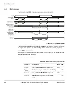
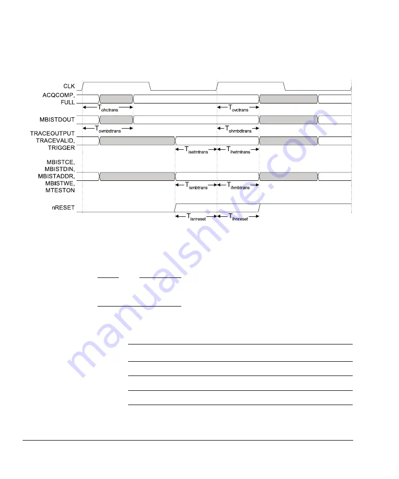
The timings for the 

CLK

 domain signals are shown in Figure 4-2.

Figure 4-2 CLK domain signals

The timing requirements for the 

CLK

 domain signals are listed in Table 4-2. All figures 

are expressed as percentages of the 

CLK

 period at maximum operating frequency.

Note

 A 0% figure in Table 4-2 indicates the hold time to clock edge plus the maximum clock 
skew for internal clock buffering.

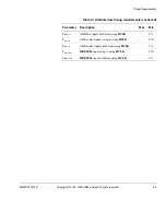
Table 4-2 CLK domain timing requirements

Parameter

Description

Max

Min

T

ovctrans

Rising 

CLK

 to 

CLK

 domain outputs valid

40%

-

T

ohctrans

CLK

 domain outputs hold time from 

CLK

 rising

>0%

T

ovmbdtrans

Rising 

CLK

 to 

MBISTDOUT

 output valid

60%

-

T

ohmbdtrans

MBISTDOUT

 output hold time from 

CLK


rising

-

>0%

Содержание ETB11

Страница 1: ...Copyright 2002 2003 ARM Limited All rights reserved ARM DDI 0275D ETB11 Revision r0p1 Technical Reference Manual ...

Страница 2: ...all warranties implied or expressed including but not limited to implied warranties of merchantability or fitness for purpose are excluded This document is intended only to assist the reader in the use of the product ARM Limited shall not be liable for any loss or damage arising from the use of any information in this document or any error or omission in such information or any incorrect use of th...

Страница 3: ...bedded Trace Buffer 1 2 1 2 ETM versions and variants 1 5 1 3 Silicon revision 1 6 Chapter 2 Functional Description 2 1 Functional information 2 2 2 2 Operation 2 4 2 3 Control logic 2 6 2 4 Data Formatter 2 8 2 5 Trigger delay counter 2 9 2 6 Address generation 2 10 2 7 BIST interface 2 11 2 8 TAP controller 2 12 2 9 Trace RAM interface 2 15 2 10 Clocks and resets 2 17 2 11 AHB transfers 2 19 ...

Страница 4: ...s to the ETB11 using the AHB interface 3 11 Chapter 4 Timing Requirements 4 1 AHB interface 4 2 4 2 CLK domain 4 4 4 3 IEEE1149 1 interface 4 6 Appendix A Signal Descriptions A 1 Signal properties and requirements A 2 A 2 Signal descriptions A 3 Appendix B Integrating the ETB11 B 1 ASIC connections B 2 B 2 Connecting to ETM11RV B 3 B 3 Connecting the ETB11 in a 64 bit AHB system B 4 Glossary ...

Страница 5: ...ble 3 5 Status Register bit allocations 3 6 Table 3 6 RAM Data Register bit allocations 3 7 Table 3 7 RAM Read Pointer Register bit allocations 3 7 Table 3 8 RAM Write Pointer Register bit allocations 3 8 Table 3 9 Trigger Counter Register bit allocations 3 9 Table 3 10 Control Register bit allocations 3 10 Table 3 11 Registers that require software access 3 11 Table 4 1 AHB interface timing requi...

Страница 6: ...List of Tables vi Copyright 2002 2003 ARM Limited All rights reserved ARM DDI 0275D ...

Страница 7: ...access from Trace RAM timing diagram 2 16 Figure 2 6 Write access to Trace RAM timing diagram 2 16 Figure 2 7 Example synchronizer 2 17 Figure 2 8 Synchronization logic between HCLK and CLK domains 2 20 Figure 2 9 Software read cycle with asynchronous CLK and HCLK 2 21 Figure 2 10 Software read cycle with synchronous CLK and HCLK 2 22 Figure 2 11 Software write cycle with asynchronous CLK and HCLK...

Страница 8: ...List of Figures viii Copyright 2002 2003 ARM Limited All rights reserved ARM DDI 0275D ...

Страница 9: ...002 2003 ARM Limited All rights reserved ix Preface This preface introduces the ARM11 Embedded Trace Buffer ETB11 Technical Reference Manual It contains the following sections About this document on page x Feedback on page xiv ...

Страница 10: ...software engineers who want to design or obtain trace information from chips that use ARM cores with the ETM facility Using this manual This document is organized into the following chapters Chapter 1 Introduction Read this chapter for an overview of the ETB11 Chapter 2 Functional Description Read this chapter for a description of the major functional blocks configurability read and write timing i...

Страница 11: ... as menu names Denotes ARM processor signal names Also used for terms in descriptive lists where appropriate monospace Denotes text that you can enter at the keyboard such as commands file and program names and source code monospace Denotes a permitted abbreviation for a command or option You can enter the underlined text instead of the full command or option name monospace italic Denotes argument...

Страница 12: ...serted means HIGH for active HIGH signals and LOW for active LOW signals Prefix A Denotes Advanced eXtensible Interface AXI global and address channel signals Prefix B Denotes AXI write response channel signals Prefix C Denotes AXI low power interface signals Prefix H Denotes Advanced High performance Bus AHB signals Prefix n Denotes Active LOW signals except in the case of AHB or Advanced Periphe...

Страница 13: ... Asked Questions ARM publications This document contains information that is specific to the ETB11 Refer to the following documents for other relevant information ETB11 Implementation Guide ARM DII 0067 Embedded Trace Buffer Rev 0 Technical Reference Manual ARM DDI 0242B Embedded Trace Macrocell Specification ARM IHI 0014 ETM11RV Technical Reference Manual ARM DDI 0233 ETM11RV Implementation Guide...

Страница 14: ...uggestions about this product contact your supplier giving the product name a concise explanation of your comments Feedback on this document If you have any comments on about this document send email to errata arm com giving the document title the document number the page number s to which your comments refer a concise explanation of your comments General suggestions for additions and improvements...

Страница 15: ...s reserved 1 1 Chapter 1 Introduction This chapter introduces the Embedded Trace Buffer ETB11 and its features It contains the following sections About the Embedded Trace Buffer on page 1 2 ETM versions and variants on page 1 5 Silicon revision on page 1 6 ...

Страница 16: ...come a very large number of trace port pins The solution is to provide a buffer area on chip where the trace information is stored and read from the chip later at a slower rate The ETB11 stores data produced by the ETM11RV The buffered data can then be accessed by the debugging tools using a JTAG IEEE 1149 1 interface as shown in Figure 1 1 Figure 1 1 System on Chip debug implementation System on ...

Страница 17: ... the information from the trace port to a debugging tool for example a PC The debug tool retrieves data from the interface unit reconstructs a historical view of processor activity including data accesses configures the macrocell through the JTAG interface unit and port User definable filters enable you to limit the amount of information captured in search of a bug reducing upload time from the tr...

Страница 18: ...75D JTAG interface unit Boundary scan is a methodology enabling complete controllability and observability of the boundary pins of a JTAG compatible device by software control This capability enables in circuit testing without requiring specially designed in circuit test equipment ...

Страница 19: ... ETM protocols it is intended for use with ETM11RV only For this reason this document only describes details related to storing trace from ETM11RV For details on using an ETB with other ETM products see the Embedded Trace Buffer Technical Reference Manual The history of the ETM is listed in Table 1 1 Table 1 1 ETM major architecture versions Name Major architecture version ETM7 ETMv1 ETM9 ETMv1 ET...

Страница 20: ...ght 2002 2003 ARM Limited All rights reserved ARM DDI 0275D 1 3 Silicon revision This manual is for ETB11 r0p1 ETB11 r0p1 includes corrections for errata in ETB11 r0p0 Further information can be found in the ETB11 errata list ...

Страница 21: ...contains the following sections Functional information on page 2 2 Operation on page 2 4 Control logic on page 2 6 Data Formatter on page 2 8 Trigger delay counter on page 2 9 Address generation on page 2 10 BIST interface on page 2 11 TAP controller on page 2 12 Trace RAM interface on page 2 15 Clocks and resets on page 2 17 AHB transfers on page 2 19 ...

Страница 22: ...e RAM interface is specified but the RAM block must be supplied by the system integrator The RAM interface is described in Trace RAM interface on page 2 15 Connection of the AHB interface is optional If you do not require software access to the ETB registers or trace RAM the AHB interface can be left unconnected If this is done all accesses to the ETB must be performed using the JTAG interface A b...

Страница 23: ...ignals Register control Reg Sync TAP controller Configuration Status TraceCaptEn nDBGTRST DBGTCKEN DBGTCK DBGTDO DBGTDI DBGTMS ReadAddrUp ReadAddrInc Addr RAW 1 0 A Trace RAM interface A CData nRESET CLK PORTSIZE 2 0 TRACEOUTPUT RBW 1 0 TRACEVALID TRIGGER PROTOCOL 1 0 Data Formatter DataValid WriteData RBW 1 0 Din D Triggered AcqComp control reg Dout RBW 1 0 Dout Q nR W WR RAMAccess CS OEN WEN CEN...

Страница 24: ...tools through the TAP controller can read trace data stored in the trace RAM through the TAP controller or through the AHB interface To read data through the TAP controller you must 1 Disable trace capture If trace capture is enabled when the RAM Data Register is accessed the RAM value read is incorrect 2 Write the location that data is read from into the RAM Read Pointer Register 3 Read the RAM D...

Страница 25: ...yright 2002 2003 ARM Limited All rights reserved 2 5 6 There are three internal status signals AcqComp Triggered Full These can be read at any time while trace capture is in progress The status signals are cleared when TraceCaptEn is cleared ...

Страница 26: ...d TrgDelayCounter is nonzero TraceCaptEn directly selects RAM write or read mode and the RAM address source When TraceCaptEn is asserted all RAM access cycles are writes using the write pointer as the address When TraceCaptEn is deasserted RAM accesses are controlled by the AHB interface when SoftwareCntl control register bit 4 is HIGH and SWEN is HIGH Otherwise all access cycles are reads using t...

Страница 27: ... ARM DDI 0275D Copyright 2002 2003 ARM Limited All rights reserved 2 7 Figure 2 3 Trace read operation CLK TraceCaptEn R R 1 UR UR 1 RAMAddr ReadData RAMAccess RegAccess Read Write ControlState D D 1 UD UD 1 ReadAddInc Read ...

Страница 28: ...ack the trace data from ETMv1 ETMs It is not used by ETM11RV Trace data is written to the trace RAM one word at a time when TRACEVALID is asserted by the ETM11RV You must set the port size to 32 bits and port mode to dynamic in the ETM11RV otherwise Unpredictable behavior might occur while using the ETB11 See the ETM Specification for details ...

Страница 29: ...ables the trigger delay counter which decrements every time a data word is written into the trace RAM When TrgDelayCounter reaches zero the acquisition complete flag AcqComp is asserted This prevents further writes to the trace RAM The AcqComp flag is cleared when trace capture is disabled TraceCaptEn 0 The state of the triggered flag can be read from the Status Register The Triggered flag is clea...

Страница 30: ... at any time However if the TAP controller clock DBGTCK is asynchronous to CLK the value might be indeterminate if read while trace capture is enabled Therefore the pointer must be accessed when TraceCaptEn is deasserted The RAM Write Pointer Register is not affected by AHB writes to the RAM 2 6 2 Read address generation When trace capture and software access to registers are disabled the RAM Read...

Страница 31: ...rovided that the TetraMax has access to a model of the RAM used Greater than 99 stuck at fault coverage can be achieved A block diagram of the BIST interface is shown in Figure 2 4 Figure 2 4 BIST interface block diagram The MTESTON signal gives an external BIST controller access to the inputs and outputs of the ETB11 RAM It is not possible for the ETB11 to operate in functional mode when the BIST...

Страница 32: ...ge 2 13 2 8 1 Test data registers There are two test data registers that can be connected between DBGTDI and DBGTDO They are described in Bypass Register Scan chain 0 on page 2 13 Bypass Register This is a single bit register that can be selected as the path between DBGTDI and DBGTDO to enable the device to be bypassed during boundary scan testing When the BYPASS instruction is the current instruc...

Страница 33: ...blic instructions listed in Table 2 1 are supported Table 2 1 Supported public instructions Instruction Binary code Description SCAN_N b0010 SCAN_N connects the 5 bit scan chain selection register between DBGTDI and DBGTDO INTEST b1100 INTEST connects the scan register selected by the scan chain selection register between DBGTDI and DBGTDO Only scan chain 0 is implemented Scan chain 0 is used to a...

Страница 34: ...hts reserved ARM DDI 0275D 2 8 3 Asynchronous clocks and testing in ETB11 ETB11 contains three clocking domains CLK DBGTCK HCLK CLK and DBGTCK can be asynchronous or synchronous ETM11RV does not have DBGTCK but uses CLK and DBGTCKEN to gate the flops in the JTAG block ...

Страница 35: ...in Table 2 2 The timing requirements for the ETB11 are described in Chapter 4 Timing Requirements 2 9 2 Read access A timing diagram showing a read access from the Trace RAM to the Trace RAM interface is shown in Figure 2 5 on page 2 16 Table 2 2 Trace RAM interface signals Signal Description CLK Clock A A configurable width address bus CE An active HIGH chip enable signal WE An active HIGH write ...

Страница 36: ...0275D Figure 2 5 Read access from Trace RAM timing diagram 2 9 3 Write access A timing diagram showing a write access to the Trace RAM from the Trace RAM interface is shown in Figure 2 6 Figure 2 6 Write access to Trace RAM timing diagram CLK CS WE A Din A1 D1 CLK CS WE A Din D1 A1 Dout D1 ...

Страница 37: ... be synchronous or asynchronous to CLK depending on your system design Synchronization logic is provided for asynchronous designs Register read and write accesses and RAM read and write accesses using the AHB interface are described in Read transfer on page 2 19 Write transfer on page 2 22 2 10 2 Resets There are the following resets nRESET resets all of the ETB11 registers in the CLK domain nRESE...

Страница 38: ...Functional Description 2 18 Copyright 2002 2003 ARM Limited All rights reserved ARM DDI 0275D HRESETn is the AHB interface reset signal and is used to reset all of the registers in the AHB interface ...

Страница 39: ...to form CReq When CReq goes HIGH the address value on HADDRReg the registered version of HADDR that remains valid until HReq goes LOW is valid The CS and CRegRead signals that control read access of the ETB11 RAM and the ETB11 registers go HIGH for one cycle after CReq goes HIGH Data is returned from the ETB11 RAM or the ETB11 registers and registered into CData CAck goes HIGH to indicate that the...

Страница 40: ...A software read cycle with HCLK and CLK asynchronous is shown in Figure 2 9 on page 2 21 In synchronous designs where HCLK is derived from CLK HCLKEN is used to control the generation of HCLK and CLK is connected to the HCLK input of the ETB11 HSel HCLK CAck HReq CReq1 CReq2 CLK HAck2 also HAck HAck1 HCLK CReq CAck D Q Q D Q Q D Q Q D Q Q D Q Q D Q Q D Q Q ...

Страница 41: ...FunctionalDescription ARM DDI 0275D Copyright 2002 2003 ARM Limited All rights reserved 2 21 Figure 2 9 Software read cycle with asynchronous CLK and HCLK ...

Страница 42: ...l is HIGH A software read cycle with CLK and HCLK synchronous is shown in Figure 2 9 on page 2 21 The pipelined nature of the ETB11 data means that data takes more than a single cycle to perform a read and write operation Wait states are inserted until the read cycle is completed Figure 2 10 Software read cycle with synchronous CLK and HCLK 2 11 2 Write transfer Two types of write transfer are des...

Страница 43: ...Req goes HIGH to perform the write access CAck then goes HIGH one cycle after CReq goes HIGH to indicate that the write data has been used in the CLK domain At the same time that HAck goes HIGH HREADYMEM goes HIGH indicating to the AHB bus master that the data has been written to its destination HReq then goes LOW indicating that the AHB transfer has finished This in turn causes CAck to go LOW one...

Страница 44: ...ARM Limited All rights reserved ARM DDI 0275D Figure 2 11 Software write cycle with asynchronous CLK and HCLK Synchronous HCLK and CLK Software write cycles with CLK and HCLK synchronous the SBYPASS signal is HIGH is shown in Figure 2 12 on page 2 25 ...

Страница 45: ...FunctionalDescription ARM DDI 0275D Copyright 2002 2003 ARM Limited All rights reserved 2 25 Figure 2 12 Software write cycle with synchronous CLK and HCLK ...

Страница 46: ...Functional Description 2 26 Copyright 2002 2003 ARM Limited All rights reserved ARM DDI 0275D ...

Страница 47: ...mer s Model This chapter describes the ETB11 registers and provides details required when programming the buffer It contains the following sections About the programmer s model on page 3 2 Register descriptions on page 3 4 Software access to the ETB11 using the AHB interface on page 3 11 ...

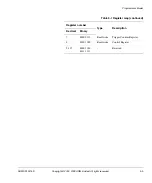
Страница 48: ...xt All registers bits are reset to a logic 0 by a reset unless otherwise stated in the relevant text All registers support read and write accesses unless otherwise stated in the relevant text A write updates and a read returns the contents of the register 3 1 2 Register map The ETB11 register map is shown in Table 3 1 Table 3 1 Register map Register number Type Description Decimal Binary 0 b000 00...

Страница 49: ...2 2003 ARM Limited All rights reserved 3 3 7 b000 0111 Read write Trigger Counter Register 8 b000 1000 Read write Control Register 9 127 b000 1001 b111 1111 Reserved Table 3 1 Register map continued Register number Type Description Decimal Binary ...

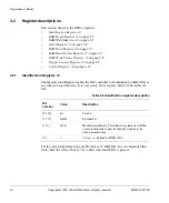
Страница 50: ...3 10 3 2 1 Identification Register r0 The Identification Register enables the TAP controller to be identified by Multi ICE or any other run control device It is a read only 32 bit register Table 3 2 describes the bits For the current implementation the ID value is 32 h2B900F0F It is recommended that tools check the value of bits 27 1 to detect that the ETB11 is present Table 3 2 Identification reg...

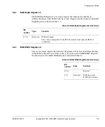
Страница 51: ...s is a read only register that indicates the number of bits in each addressable entry in the RAM to the trace tools This is always 32 when used with ETM11RV Register bit allocations for the RAM Width Register are listed in Table 3 4 Table 3 3 RAM Depth Register bit allocations Bit number Type Function 31 0 Read only RAM data depth This value is configurable in the RTL but must be fixed when the ET...

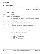
Страница 52: ...s set 6 Read the trace Table 3 5 Status Register bit allocations Bit number Name Function 31 4 Reserved 3 DFEmpty Data Formatter pipeline empty This bit is required because when tracing is disabled there might still be some trace data in the Data Formatter pipeline This is drained within a few cycles after trace capture is disabled see Control Register r8 on page 3 10 You can ensure that all trace...

Страница 53: ...ce because the RAM is memory mapped See Software access to the ETB11 using the AHB interface on page 3 11 3 2 6 RAM Read Pointer Register r5 This read write register enables you to set and read the pointer used to read entries from the RAM Register bit allocations for the RAM Read Pointer Register are listed in Table 3 7 Note ETB_ADDR_WIDTH is a constant used to define the width of the trace RAM a...

Страница 54: ... initial value of the trace memory write address pointer is set by writing to the RAM Write Pointer Register You must program the pointer before tracing starts In most circumstances the initial pointer value is zero During trace capture the pointer increments when the DataValid flag is asserted by the Data Formatter When the RAM Write Pointer Register value increments from its maximum value back t...

Страница 55: ...ed to define the width of the trace RAM address bus When written the value of the Trigger Counter Register is set You must update this register before enabling trace capture failure to do so can result in unexpected trace behavior Reading the Trigger Counter Register samples the value of the trigger counter During trace capture the value of the counter can change at any time Therefore if a read is...

Страница 56: ...s up from reset with the SoftwareCntl bit enabled The value of this bit can only be changed through the TAP controller It is cleared when the INTEST instruction is selected by the TAP controller and is set by writing a 1 as normal While this bit is clear all accesses to the register by the AHB interface are ignored Table 3 10 Control Register bit allocations Bit number Name Type Function 31 3 Rese...

Страница 57: ... 1 This is the default and is set to 1 on reset Additionally software access to ETB11 RAM is only enabled when bit 0 of the control register is set to 0 ETB11 is enabled The interface contains an input signal called SWEN When this signal is LOW the interface is disabled The AHB interface is enabled if SWEN is HIGH Table 3 11 Registers that require software access Register number Description Locati...

Страница 58: ...ce to read trace data the following are not permitted byte or halfword accesses when the memory does not support them unaligned accesses transfers larger than a word for example 64 bit transfers Only aligned single word accesses are permitted Register access supports aligned single word accesses only Use of the AHB interface as system memory requires careful system design to ensure that the memory...

Страница 59: ...All rights reserved 4 1 Chapter 4 Timing Requirements The timing requirements for the ETB11 interfaces are defined in this chapter It contains the following sections AHB interface on page 4 2 CLK domain on page 4 4 IEEE1149 1 interface on page 4 6 ...

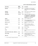
Страница 60: ...dicates the hold time to clock edge plus the maximum clock skew for internal clock buffering Tihhresetn Tishresetn Tihhcon Tishcon Tihhdata Tishdata Tohhcon Tovhcon Tohhdata Tovhdata HADDR HWDATA HRDATAMEM HCLK HRESP HREADYMEM HWRITE HTRANS HSIZE HREADY HSELREG HSELMEM HRESETn Table 4 1 AHB interface timing requirements Parameter Description Max Min Tovhdata Rising HCLK to HRDATAMEM valid 40 Tohhd...

Страница 61: ...uts hold from rising HCLK 0 Tishcon AHB control inputs setup to rising HCLK 30 Tihhcon AHB control inputs hold from rising HCLK 0 Tishresetn HRESETn input setup to rising HCLK 30 Tihhresetn HRESETn input hold from rising HCLK 0 Table 4 1 AHB interface timing requirements continued Parameter Description Max Min ...

Страница 62: ...e expressed as percentages of the CLK period at maximum operating frequency Note A 0 figure in Table 4 2 indicates the hold time to clock edge plus the maximum clock skew for internal clock buffering Table 4 2 CLK domain timing requirements Parameter Description Max Min Tovctrans Rising CLK to CLK domain outputs valid 40 Tohctrans CLK domain outputs hold time from CLK rising 0 Tovmbdtrans Rising C...

Страница 63: ...40 Tihmbtrans MBIST inputs hold from rising CLK 0 Tisetmtrans ETM interface inputs setup to rising CLK 40 Tihetmtrans ETM interface inputs hold from rising CLK 0 Tisnreset nRESET input setup to rising CLK 40 Tihnreset nRESET input hold from rising CLK 0 Table 4 2 CLK domain timing requirements continued Parameter Description Max Min ...

Страница 64: ...the DBGTCK period at maximum operating frequency Note A 0 figure in Table 4 3 indicates the hold time to clock edge plus the maximum clock skew for internal clock buffering Table 4 3 IEEE1149 1 interface timing requirements Parameter Description Max Min Tovttrans Rising DBGTCK to DBGTDO output valid 40 Tohttrans DBGTDO output hold time from DBGTCK rising 0 Tisttrans JTAG inputs setup to rising DBG...

Страница 65: ...M Limited All rights reserved A 1 Appendix A Signal Descriptions This appendix describes the ETB11 input and output signals It contains the following sections Signal properties and requirements on page A 2 Signal descriptions on page A 3 ...

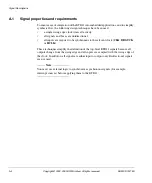
Страница 66: ...l signals and buses are unidirectional all inputs are required to be synchronous to the relevant clock CLK DBGTCK or HCLK These techniques simplify the definition of the top level ETB11 signals because all outputs change from the rising edge and all inputs are sampled with the rising edge of the clock In addition all signals are either input or output only Bidirectional signals are not used Note Y...

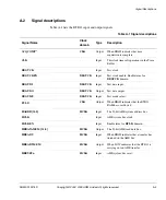
Страница 67: ...st clock enable Enable term for DBGTCK domain DBGTDI DBGTCK Input Test data input DBGTDO DBGTCK Output Test data output DBGTMS DBGTCK Input Test mode select FULLa CLK Output When HIGH indicates that the ETB11 RAM has overflowed HADDR 31 0 HCLK Input The 32 bit AHB system address bus HCLK Input AHB system bus clock HCLKEN Input Enable term for HCLK domain HRDATAMEM 31 0 HCLK Output The 32 bit AHB r...

Страница 68: ...AHB transfer HTRANS 1 0 HCLK Input Indicates the type of AHB transfer 00 IDLE 01 BUSY 10 NONSEQ 11 SEQ HWDATA 31 0 HCLK Input The 32 bit AHB write data bus HWRITE HCLK Input When HIGH indicates an AHB write transfer When LOW indicates an AHB read transfer MBISTADDR ETB_ADDR_WIDTH 1 0 CLK Input Address Bus for external BIST controller active when MTESTON is HIGH MBISTCE CLK Input Active HIGH chip s...

Страница 69: ...TSIZE 2 0 CLK Input Indicates currently selected port size in use on the TRACEPKT 15 0 bus PROTOCOL 1 0 CLK Input Indicates the currently selected ETM protocol SBYPASS CLK Input Indicates that HCLK and CLK are synchronous so the synchronizing logic can be bypassed SCANMODE CLK Input Selects scan mode SE CLK Input Scan enable SWEN Input When LOW disables software access to the ETB11 TRACEOUTPUT ETB...

Страница 70: ...Signal Descriptions A 6 Copyright 2002 2003 ARM Limited All rights reserved ARM DDI 0275D ...

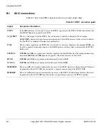
Страница 71: ...ix B Integrating the ETB11 This section describes how to integrate the ETB11 if you are not using the ETK11 Integration Kit It contains the following sections ASIC connections on page B 2 Connecting to ETM11RV on page B 3 Connecting the ETB11 in a 64 bit AHB system on page B 4 ...

Страница 72: ...at can be used to control on chip logic For example FULL can be used to generate an interrupt request to the ARM processor in the system to indicate that the ETB11 RAM is full SBYPASS If HCLK and CLK are synchronous then this signal must be tied HIGH so that the synchronization logic between the HCLK and CLK domain is bypassed Otherwise this must be tied LOW HCLK If HCLK and CLK are synchronous th...

Страница 73: ...eme listed in Table B 2 to connect the ETB11 to a generic trace port interface device such as an ETM11RV Table B 2 ETB11 to generic trace port interface connections ETB11 signal Connection to ETM11RV TRACEOUTPUT 31 0 TRACEDATA 31 0 TRACEVALID TRACEVALID TRIGGER TRIGGER PROTOCOL 1 0 b10 PORTSIZE 2 0 PORTSIZE 2 0 DBGTCK CLK DBGTCKEN DBGTCKEN ...

Страница 74: ...WDATAMEM 31 0 Recreate the 64 bit bus from the 32 bit Trace Buffer HRDATA bus assign HRDATAMEM HRDATAMEM32 HRDATAMEM32 code If the code shown in Example B 1 is used then load store multiple instructions that access the ETB11 have unpredictable results because these use both halves of the 64 bit bus at the same time These accesses do not cause an AHB ERROR response which normally cause a Data Abort...

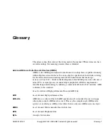
Страница 75: ...p a System on Chip SoC It aids in the development of embedded processors with one or more CPUs or signal processors and multiple peripherals AMBA complements a reusable design methodology by defining a common backbone for SoC modules AHB conforms to this standard See also Advanced High performance Bus and AHB Lite AHB See Advanced High performance Bus AHB Lite AHB Lite is a subset of the full AHB ...

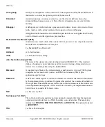
Страница 76: ...ion Group Joint Test Action Group JTAG The name of the organization that developed standard IEEE 1149 1 This standard defines a boundary scan architecture used for in circuit testing of integrated circuit devices It is commonly known by the initials JTAG Macrocell A complex logic block with a defined interface and behavior A typical VLSI system comprises several macrocells such as an ETM9 and a me...

Страница 77: ...he analyzer reconstruct an historical view of the processor s activity including data accesses as well as configuring the macrocell using the JTAG port Powerful user definable filters enable you to limit the amount of information captured in search of a bug reducing upload time from the trace port analyzer Unpredictable For reads the data returned when reading from this location is unpredictable I...

Страница 78: ...Glossary Glossary 4 Copyright 2002 2003 ARM Limited All rights reserved ARM DDI 0275D ...

Страница 79: ...4 C CLK domain 4 4 Clock domains 2 17 Clocks 2 17 Configurability 2 2 Control logic 2 6 Control Register 3 10 Conventions numerical xiii signal naming xii timing diagram xii typographical xi D Data formatter 2 8 Debug implementation 1 2 Design techniques ETB11 A 2 E EmbeddedICE 1 3 ETB11 design techniques A 2 module 2 2 ETM 1 3 ETMv3 generic trace port interface B 3 G Generic trace port interface ...

Страница 80: ... A 3 DBGTCKEN A 3 DBGTDI A 3 DBGTMS A 3 FULL A 3 B 2 HADDR A 3 HCLK A 3 B 2 HCLKEN A 3 B 2 HRDATAMEM A 3 HREADY A 3 HREADYMEM A 3 HRESETn A 3 HRESPMEM A 4 HSELMEM A 4 B 2 HSELREG A 4 B 2 HSIZE A 4 HTRANS A 4 HWDATA A 4 B 4 HWRITE A 4 MBISTADDR A 4 MBISTCE A 4 MBISTDIN A 4 MBISTDOUT A 4 MBISTWE A 5 MTESTON A 5 nDBGTDOEN A 5 nDBGTRST A 5 nRESET A 5 PORTSIZE A 5 B 3 PROTOCOL A 5 B 3 SBYPASS A 5 B 2 S...

Отзывы: