background image

Signal Descriptions 

ARM DDI 0186A

Copyright © 2000 ARM Limited. All rights reserved.

A-15

A.9

DMA Signals

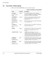
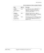
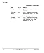
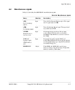
DMA signals are listed in Table A-8.

Table A-8 DMA signals

Name

Direction

Description

DMAENABLE

Input

Enable ARM966E-S DMA port. Must be tied LOW 
if DMA not required.

DMAnREQ

Input

DMA not memory request. Must be tied HIGH if 
DMA not required.

DMAA[25:0]

Input

DMA address. Accesses up to 64Mbyte of memory. 
Unused address bits must be tied LOW.

DMAnRW

Input

DMA write not read:

0 = read

1 = write.

DMAMAS[1:0]

Input

DMA Memory Access Size. Encodes the size of 
writes. Reads are always word wide:

00 = byte

01 = halfword

10 = word

11 = reserved.

DMAD[31:0]

Input

DMA write data.

DMAWait

Input

DMA Wait. Used to stall the ARM966E-S to allow a 
DMA access to take place. This functionality is only 
required if the data RAM is single-port. This signal 
must be tied LOW if the data RAM is dual-port.

This signal has the same functionality internal to the 
ARM966E-S as 

FIFOFULL

.

DMAReady

Output

DMA Ready. Asserted HIGH when the ARM966E-S 
is stalled. Only needs to be sampled when the data 
RAM is single port, for example when the 
ARM966E-S stall was requested by 

DMAWait

.

DMARData[31:0]

Output

DMA read data.

Содержание ARM966E-S

Страница 1: ...Copyright 2000 ARM Limited All rights reserved ARM DDI 0186A ARM966E S Rev 1 Technical Reference Manual ...

Страница 2: ... use contained in this document are given by ARM in good faith However all warranties implied or expressed including but not limited to implied warranties of merchantability or fitness for purpose are excluded This document is intended only to assist the reader in the use of the product ARM Limited shall not be liable for any loss or damage arising from the use of any information in this document ...

Страница 3: ...S 1 2 1 2 Microprocessor block diagram 1 3 Chapter 2 Programmer s Model 2 1 About the programmer s model 2 2 2 2 About the ARM9E S programmer s model 2 3 2 3 ARM966E S CP15 registers 2 4 Chapter 3 Memory Map 3 1 About the ARM966E S memory map 3 2 3 2 Tightly coupled SRAM address space 3 3 3 3 Bufferable write address space 3 4 Chapter 4 Tightly coupled SRAM 4 1 ARM966E S SRAM requirements 4 2 4 2 ...

Страница 4: ... 7 5 CDP 7 10 7 6 Privileged instructions 7 11 7 7 Busy waiting and interrupts 7 12 Chapter 8 Debug Support 8 1 About the debug interface 8 2 8 2 Debug systems 8 4 8 3 ARM966E S scan chain 15 8 7 8 4 Debug interface signals 8 9 8 5 ARM9E S core clock domains 8 14 8 6 Determining the core and system state 8 15 8 7 About the EmbeddedICE RT 8 16 8 8 Disabling EmbeddedICE RT 8 18 8 9 The debug communi...

Страница 5: ...errupt latency calculation 11 10 Appendix A Signal Descriptions A 1 Signal properties and requirements A 2 A 2 Clock interface signals A 3 A 3 AHB signals A 4 A 4 Coprocessor interface signals A 6 A 5 Debug signals A 8 A 6 Miscellaneous signals A 11 A 7 ETM interface signals A 12 A 8 INTEST wrapper signals A 14 A 9 DMA Signals A 15 Appendix B AC Parameters B 1 Timing diagrams B 2 B 2 AC timing par...

Страница 6: ...Contents vi Copyright 2000 ARM Limited All rights reserved ARM DDI 0186A ...

Страница 7: ... Table 4 1 I SRAM stall cycles 4 3 Table 5 1 Simultaneous access behavior 5 3 Table 5 2 DMAENABLE setup and hold cycles with respect to DMAnREQ 5 11 Table 5 3 DMA signal behavior 5 12 Table 7 1 Handshake encoding 7 6 Table 8 1 Scan chain 15 addressing mode bit order 8 7 Table 8 2 Mapping of scan chain 15 address field to CP15 registers 8 7 Table 8 3 Coprocessor 14 register map 8 19 Table 10 1 Inst...

Страница 8: ...y 11 10 Table 11 7 Interrupt latency calculated examples 11 11 Table A 1 Clock interface signals A 3 Table A 2 AHB signals A 4 Table A 3 Coprocessor interface signals A 6 Table A 4 Debug signals A 8 Table A 5 Miscellaneous signals A 11 Table A 6 ETM interface signals A 12 Table A 7 INTEST wrapper signals A 14 Table A 8 DMA signals A 15 Table B 1 AC parameters B 12 ...

Страница 9: ...DMA interface 5 3 Figure 5 2 Dual port RAM DMA interface 5 4 Figure 5 3 Single port RAM DMA reads 5 5 Figure 5 4 Single port RAM DMA writes 5 7 Figure 5 5 Dual port DMA reads 5 8 Figure 5 6 Dual port RAM DMA writes 5 9 Figure 5 7 Mixed DMA read and write 5 10 Figure 6 1 Write buffer FIFO content example 6 4 Figure 6 2 Sequential instruction fetches after being granted the bus 6 8 Figure 6 3 Sequen...

Страница 10: ...8 12 Figure 8 7 The ARM9E S TAP controller and EmbeddedICE RT 8 16 Figure 8 8 Debug communications channel status register 8 20 Figure 8 9 Coprocessor 14 debug status register format 8 21 Figure 9 1 ARM966E S ETM interface 9 2 Figure B 1 Clock reset and AHB enable timing B 2 Figure B 2 AHB bus request and grant related timing B 3 Figure B 3 AHB bus master timing B 4 Figure B 4 Coprocessor interfac...

Страница 11: ...0 ARM Limited All rights reserved xi Preface This preface introduces the ARM966E S and its reference documentation It contains the following sections About this document on page xii Further reading on page xv Feedback on page xvi ...

Страница 12: ... S coprocessor registers Chapter 3 Memory Map Read this chapter for a description of the ARM966E S fixed memory map implementation Chapter 4 Tightly coupled SRAM Read this chapter for a description of the requirements and operation of the tightly coupled SRAM Chapter 5 Direct Memory Access DMA Read this chapter for a description of the optional DMA interface in the ARM966E S Chapter 6 Bus Interfac...

Страница 13: ...pendix for a description of the tightly coupled SRAM stall cycle mechanism in the ARM966E S Typographical The typographical conventions are italic Highlights important notes introduces special terminology denotes internal cross references and citations bold Highlights interface elements such as menu names Denotes signal names Also used for terms in descriptive lists where appropriate monospace Den...

Страница 14: ...f timing diagrams The following key explains the components used in these diagrams Any variations are clearly labeled when they occur Therefore no additional meaning should be attached unless specifically stated Key to timing diagram conventions Shaded bus and signal areas are undefined so the bus or signal can assume any value within the shaded area at that time The actual level is unimportant an...

Страница 15: ...e questions not answered by this document please contact info arm com or visit our web site at http www arm com ARM publications ARM Architecture Reference Manual ARM DDI 0100 ARM9E S Technical Reference Manual ARM DDI 0165 AMBA Specification Rev 2 0 ARM IHI 0011 AHB Example AMBA System Technical Reference Manual ARM DDI 0170 Other publications IEEE Std 1149 1 1990 Standard Test Access Port and Bo...

Страница 16: ...ons about this product please contact your supplier giving the product name a concise explanation of your comments Feedback on the ARM966E S If you have any comments about this document please send e mail to errata arm com giving the document title the document number the page number s to which your comments refer a concise explanation of your comments General suggestions for additions and improve...

Страница 17: ...ht 2000 ARM Limited All rights reserved 1 1 Chapter 1 Introduction This chapter introduces the ARM966E S processor It contains the following sections About the ARM966E S on page 1 2 Microprocessor block diagram on page 1 3 ...

Страница 18: ...ze of both the instruction and data SRAM are implementor configurable to allow tailoring of the hardware to the embedded application Additionally You can configure the data SRAM interface to allow Direct Memory Access DMA to this RAM The ARM9E S core within the ARM966E S macrocell executes both the 32 bit ARM and 16 bit Thumb instruction sets allowing trade off between high performance and high co...

Страница 19: ...is shown in Figure 1 1 Figure 1 1 ARM966E S block diagram ARM9E S Instruction SRAM Data SRAM System control coprocessor CP15 External coprocessor interface AHB Bus Interface Unit and write buffer System controller ETM interface IA DA WDATA RDATA INSTR Addr Din Addr Din Dout Dout DMA interface AHB Peripherals DMA Controller ETM Coprocessors ...

Страница 20: ...Introduction 1 4 Copyright 2000 ARM Limited All rights reserved ARM DDI 0186A ...

Страница 21: ...d 2 1 Chapter 2 Programmer s Model This chapter describes the programmer s model for the ARM966E S It contains the following sections About the programmer s model on page 2 2 About the ARM9E S programmer s model on page 2 3 ARM966E S CP15 registers on page 2 4 ...

Страница 22: ...ors within the ARM966E S CP14 within the ARM9E S core allows software access to the debug communications channel CP15 allows configuration of the tightly coupled SRAM and write buffer and other ARM966E S system options such as big or little endian operation The registers defined in CP14 are accessible with MCR and MRC instructions These are described in The debug communications channel on page 8 1...

Страница 23: ...rom the base updated data abort model implemented by ARM7TDMI The difference in the Data Abort model affects only a very small section of operating system code the Data Abort handler It does not affect user code With the base restored data abort model when a Data Abort exception occurs during the execution of a memory access instruction the base register is always restored by the processor hardwar...

Страница 24: ... on page 2 5 Register 7 Core control on page 2 7 Register 15 Test on page 2 9 2 3 1 CP15 register map summary The ARM966E S incorporates CP15 for system control The register map for CP15 is shown in Table 2 1 Note Register 15 provides access to more than one register The register access depends on the value of the opcode_2 field See the register descriptions in this section for more information Ta...

Страница 25: ...e Table 2 3 All reserved bits must either be written with zero or one as indicated or written using read modify write The reserved bits have an unpredictable value when read To read and write this register MRC p15 0 rd c1 c0 0 read Control register MCR p15 0 rd c1 c0 0 write Control register Table 2 2 Register 0 ID code Register bits Function Value 31 24 Implementor 0x41 23 20 Variant 0x0 19 16 AR...

Страница 26: ...W during system reset depending on the value of the input pin VINITHI This allows the exception vector location to be defined during reset to suit the boot mechanism of the application You can then reprogram as required following system reset Bit 12 Instruction SRAM enable This bit controls the behavior of the tightly coupled instruction SRAM When HIGH all accesses to the fixed instruction memory ...

Страница 27: ...reated as buffered writes When LOW all stores to the AMBA AHB are treated as nonbufferable If the write buffer is disabled having previously been enabled any writes already in the write buffer FIFO complete as buffered writes This bit is cleared LOW during reset Bit 2 Data SRAM enable This bit controls the behavior of the tightly coupled Data SRAM When HIGH all data interface accesses to the fixed...

Страница 28: ...nabled or disabled that is independent of the I and F bits in the processor CPSR The debug related waking only occurs if DBGEN is HIGH that is only when debug is enabled If interrupts are enabled the ARM9E S core is guaranteed to take the interrupt before executing the instruction after the wait for interrupt If debug request is used to wake up the system the processor enters debug state before ex...

Страница 29: ...e 2 3 6 Register 15 Test This register provides access to the tightly coupled Instruction and Data SRAM test features the trace control features Both features are supported by the ARM966E S The register map for CP15 register 15 is shown in Table 2 5 Table 2 4 Register 13 Trace process identifier Register Read Write Trace Process Identifier MRC p15 0 Rd c13 c1 1 MCR p15 0 Rd c13 c1 1 Table 2 5 Regi...

Страница 30: ...rrupts during trace 0 Do not mask nIRQ interrupts during trace 2 1 Mask nFIQ interrupts during trace 0 Do not mask nFIQ interrupts during trace 31 3 Reserved should be zero Table 2 7 BIST control register Register bit Meaning when written Meaning when read 31 21 Instruction SRAM BIST size Instruction SRAM BIST size 20 Reserved should be zero Instruction SRAM BIST complete flag 19 Reserved should b...

Страница 31: ... the SRAM contents The BIST size field determines the size of the BIST operation The value written to this field N is decoded as follows BIST size in bytes 2N 2 Some examples are shown in Table 2 8 Note BIST size bits 31 26 should be zero 2 Data SRAM BIST enable Data SRAM BIST enable 1 Data SRAM BIST pause Data SRAM BIST pause 0 Data SRAM BIST start strobe Data SRAM BIST running flag Table 2 7 BIS...

Страница 32: ...Instruction SRAM BIST operation You can run Instruction and Data BIST operations individually or concurrently You must set up the Size Pause and Enable bits within the BIST control register prior to initiating a BIST operation Reading the BIST control register returns the status of the BIST operations See BIST of tightly coupled SRAM on page 10 4 for a detailed description of the BIST support and ...

Страница 33: ... 3 1 Chapter 3 Memory Map This chapter describes the ARM966E S fixed memory map implementation It contains the following sections About the ARM966E S memory map on page 3 2 Tightly coupled SRAM address space on page 3 3 Bufferable write address space on page 3 4 ...

Страница 34: ...em bus A write buffer is used to minimize traffic on the AHB bus To provide simple control over the SRAM and write buffer a fixed memory map is implemented within the ARM966E S Figure 3 1 illustrates this map Figure 3 1 ARM966E S memory map 256MB 256MB 256MB 128MB 64MB 64MB AHB unbuffered AHB buffered AHB unbuffered AHB buffered D SRAM I SRAM Tightly coupled SRAM AMBA AHB 0xFFFF FFFF 0xF000 0000 0...

Страница 35: ...BIU An instruction fetch from the ARM9E S core to the D SRAM address space goes to the AHB regardless of whether the D SRAM is enabled A data interface access from the ARM9E S core can access both the D SRAM and the I SRAM The ability to additionally access the I SRAM is required to allow the fetching of inline literals within code for programming of the instruction I SRAM and for debugging purpos...

Страница 36: ...ls whether the write buffer is used If bit 28 of DA is set the write is treated as un buffered If bit 28 is clear however the write is treated as a buffered write and the BIU write buffer FIFO is used Buffered writes allow the core to continue program execution while the write is performed on the AHB If the write buffer is full the core is stalled until space becomes available in the FIFO See Writ...

Страница 37: ...ightly coupled SRAM in the ARM966E S It contains the following sections ARM966E S SRAM requirements on page 4 2 SRAM stall cycles on page 4 3 Enabling the SRAM on page 4 4 ARM966E S SRAM wrapper on page 4 7 For details of the ARM9E S interface signals referenced in this section refer to the ARM9E S Technical Reference Manual ...

Страница 38: ...RAM and the instruction data is routed both to the instruction and data interfaces of the core See Figure 1 1 on page 1 3 for details of this data and address multiplexing ARM966E S supports the use of synchronous SRAM The SRAM control has been implemented in a way that expects the compiled SRAM memory cells to return read data to ARM9E S in a single cycle This requirement applies to both the I SR...

Страница 39: ...SYSCLKEN input is then de asserted until the SRAM has performed the access Table 4 1 shows the number of stall cycles added for different stall mechanisms for the I SRAM Note Data reads from the I SRAM incur a single cycle stall for each read instruction and not each separate RAM read LDM and LDR operations both incur a single stall cycle The D SRAM stall mechanism is write followed by read and th...

Страница 40: ...can then be individually or jointly enabled by writing to the CP15 control register register 1 Reset with INITRAM HIGH If however INITRAM is held HIGH during reset both SRAM blocks are enabled when the ARM966E S comes out of reset This is normally used for a warm reset where the SRAM has already been programmed before the application of nRESET to the ARM966E S In this case the SRAM contents are pr...

Страница 41: ...se several stall cycles for each access Caution Care must be taken to ensure that the I SRAM is appropriately initialized before it is enabled and used to supply instructions to the ARM9E S core If the core tries to execute instructions from uninitialized I SRAM the behavior is unpredictable Disabling the I SRAM You can disable the I SRAM by clearing bit 12 of the CP15 control register When the I ...

Страница 42: ... disable the D SRAM by clearing bit 2 of the CP15 control register When the D SRAM is disabled all further reads and writes to the D SRAM address space as shown in Figure 3 1 on page 3 2 access the AHB Read and write accesses to I SRAM address space uses the I SRAM or accesses the AHB depending on if it is enabled ...

Страница 43: ...des a standard interface to the ARM966E S SRAM control ARM provides an example SRAM wrapper containing three example interfaces see Example SRAM interfaces on page 4 8 You must study these examples and decide which is most appropriate for the type of SRAM available A script is provided which automates any required changes The RAM interface RTL allows you to trade off speed against power performanc...

Страница 44: ...ne in the IRamIF v and the DRamIF v blocks for the I SRAM and D SRAM respectively The example SRAM interfaces are ONESEGX32 FOURSEGX32 on page 4 9 FOURSEGX8 on page 4 10 Note The examples shown here are for 32KByte I SRAM 8K words x 4bytes The interface for D SRAM is identical ONESEGX32 Figure 4 3 shows the simplest interface I SRAM To use this the SRAM must consist of a single word wide RAM that ...

Страница 45: ...ance because only the segment being accessed is enabled The SRAM address is 11 bits in this example compared with the 13 bit address in ONESEGX32 on page 4 8 RamAddr 12 11 are used to generate separate chip selects for each segment If it is not possible to have separate chip select signals for each block of RAM for example if the RAM is asynchronous then separate write enable signals are required ...

Страница 46: ...plex interface possible Figure 4 5 on page 4 11 assumes that each byte wide SRAM needs to be split into four blocks see word wide SRAM in FOURSEGX32 on page 4 9 In FOURSEGX32 on page 4 9 the SRAM Address is 11 bits Bits 12 11 of the address are used to decode which of the four word wide RAMs is selected In Figure 4 5 on page 4 11 ByteWrite 3 0 is used inside IRamIF v to decode each word wide chip ...

Страница 47: ...11 Figure 4 5 FOURSEGX8 interface ICtrl v IRamIF v ChipSelect 15 0 WriteEnable RamAddr 10 0 ByteWrite 3 0 IRData 31 0 OutputSelect 1 0 0 4 8 12 1 5 9 13 2 6 10 14 2Kx8 2Kx8 2Kx8 2Kx8 2Kx8 2Kx8 2Kx8 2Kx8 2Kx8 2Kx8 2Kx8 2Kx8 2Kx8 2Kx8 2Kx8 2Kx8 3 7 11 15 Byte 1 Byte 0 Byte 2 Byte 3 8 32 ...

Страница 48: ...Tightly coupled SRAM 4 12 Copyright 2000 ARM Limited All rights reserved ARM DDI 0186A ...

Страница 49: ...Direct Memory Access DMA This chapter describes the optional DMA interface in the ARM966E S It contains the following sections About the DMA interface on page 5 2 Timing interface on page 5 5 DMAENABLE setup and hold cycles on page 5 11 Summary of signal behavior on page 5 12 ...

Страница 50: ...de Data RAM address space access Bits 31 26 however are not required to be driven by the DMA controller because DMA access is always to this address space RAM aliasing occurs for DMA access in the same way as aliasing occurs for CPU accesses See Tightly coupled SRAM address space on page 3 3 for more information Note The decision to connect to the DMA port and to a particular type of RAM is made p...

Страница 51: ...s higher performance than the single port solution but uses a larger die area The programmer must ensure that DMA and CPU do not access the same memory locations simultaneously The behavior of accessing the same memory locations simultaneously is either undefined or illegal Simultaneous access behavior is summarized in Table 5 1 Addr WriteEnable ChipSelect DataIn ByteWrite SP DMA access CPU RAM ac...

Страница 52: ... and is unlikely to be used so to prevent the core from being stalled DMAWait must be tied LOW Figure 5 2 Dual port RAM DMA interface Read Write Undefined Write Read Undefined Write Write Illegal Table 5 1 Simultaneous access behavior continued Core access DMA access behavior CPU RAM Access SP DMA Access CPU Read Data RAMRData1 CLK DMACLK SP DMA Access RAMRData2 DP DMA Access DMACLK Dual Port RAM ...

Страница 53: ...ehavior of the ARM966E S for DMA read and writes to single and dual port RAMs Note The dual port RAM DMA solution also supports the single port operation and so the single port diagrams are also applicable to dual port RAMs 5 2 1 Single port RAM reads Figure 5 3 shows DMA read operation from a single port RAM Figure 5 3 Single port RAM DMA reads CLK DMAENABLE DMAnREQ DMAWait DMAnRW DMAReady DMAAdd...

Страница 54: ...d address DMAAddr is registered by the ARM966E S on the next rising clock edge after DMAReady is asserted The DMA controller has ownership of the RAM from DMAReady being asserted until it takes DMAWait LOW When DMAWait has been taken LOW the DMA controller loses ownership of the RAM DMAWait must be taken LOW at the end of a DMA access to allow CPU flow to continue DMAENABLE must be asserted one cy...

Страница 55: ...d in the same cycle The read data DMARData is returned in the third cycle after the request is registered by the ARM966E S one cycle to register the request one cycle to read the RAM and one cycle to register the output data Note Because the ARM966E S core does not need to be stalled for dual port DMA accesses the DMA controller can access the data RAM continuously DMAWait must be tied LOW otherwi...

Страница 56: ...king DMAnREQ LOW and DMAnRW HIGH The address DMAAddr and write data DMAWData must be valid in the same cycle The write to the RAM happens in the following cycle due to the one cycle latency of the input registers Note Because the ARM966E S core does not need to be stalled for dual port DMA accesses the DMA controller can access the data RAM continuously DMAWait must be tied LOW otherwise the DMA a...

Страница 57: ... 5 6 Dual port RAM DMA writes 5 2 5 Mixed read and writes Figure 5 7 on page 5 10 shows an example of intermingled DMA read and write operations that reads and writes can be performed back to back The behavior is the same for both single and dual port RAMs Depending on whether the RAM was single or dual port the behavior of DMAENABLE DMAWait and DMAReady is described in sections Single port RAM re...

Страница 58: ...ect Memory Access DMA 5 10 Copyright 2000 ARM Limited All rights reserved ARM DDI 0186A Figure 5 7 Mixed DMA read and write CLK DMAnREQ DMAnRW DMAAddr DMAWData DMARData A1 A2 A3 A4 WD_A2 WD_A4 RD_A1 RD_A3 ...

Страница 59: ...or DMAENABLE with respect to DMAnREQ for both single and dual port RAMs To reduce power consumption DMAENABLE must be taken LOW when DMA accesses are not taking place or if DMA is not implemented Table 5 2 DMAENABLE setup and hold cycles with respect to DMAnREQ Operation Setup Hold Dual port RAM DMA read 1 1 Dual port RAM DMA write 1 0 Single port RAM DMA read 1 1 Single port RAM DMA write 1 0 ...

Страница 60: ...e ARM966E S DMAWait Input The DMA controller does not need to stall the ARM966E S and so this signal must be tied LOW external to the ARM966E S The DMA controller must drive this signal HIGH whenever it requires access to the data RAM Must be tied LOW external to the ARM966E S DMAnREQ Input Must be driven LOW by the DMA controller whenever it requires access to the data RAM Must be driven LOW by t...

Страница 61: ... 6 Bus Interface Unit This chapter describes the ARM966E S Bus Interface Unit BIU and write buffer It contains the following sections About the BIU and write buffer on page 6 2 Write buffer operation on page 6 3 AHB bus master interface on page 6 7 AHB clocking on page 6 17 ...

Страница 62: ...6E S BIU implements a fully compliant AHB bus master interface and incorporates a write buffer to increase system performance The BIU is the link between the ARM9E S core with its tightly coupled SRAM and the external AHB memory The AHB memory must be accessed to initialize the tightly coupled SRAM The AHB memory must also be accessed to access code and data that are not assigned to the tightly co...

Страница 63: ...ffer awaiting AHB access 6 2 1 Committing write data to the write buffer The write buffer is used when the following conditions are met the write buffer is enabled the address is in a bufferable region the address is in AHB external memory or the address selects a tightly coupled SRAM that is disabled For details on write buffer enable and the ARM966E S fixed address map see Register 1 Control reg...

Страница 64: ...data from the write buffer The write buffer can drain naturally where AHB writes occur whenever data is committed to the FIFO The core is only stalled if the write buffer overflows However there are times when a complete drain of the write buffer is enforced Data Address Data Data Address Data Address Data Data Data Address r7 r2 r4 r3 r13 r5 r6 r4 r3 r2 r13 A Word A Word A Byte A Word S S S From ...

Страница 65: ...that the address incrementer must be used to produce the AHB address for the second and following writes of the STM This mechanism allows only one FIFO entry to be used for the address leaving more room for data see Figure 6 1 on page 6 4 If a STM crosses a 1KB boundary the AHB specification requires that the first access in the new 1KB region is a nonsequential access This allows the BIU to have ...

Страница 66: ...y and the final write is completed on the AHB This instruction is described in Register 7 Core control on page 2 7 This instruction is useful when the software requires that a write is completed before program execution continues 6 2 3 Enabling the write buffer The write buffer can be enabled by setting bit 3 of the CP15 control register When this bit is set all writes to bufferable address locati...

Страница 67: ...nd therefore the pipelined address and control for the next access is also stretched This creates a system where all AHB masters and slaves sample HREADY on the rising edge of the HCLK to determine whether an access has completed and a new address can be sampled or driven out 6 3 2 ARM966E S transfer descriptions The ARM966E S BIU performs a subset of the possible AHB bus transfers available This ...

Страница 68: ... of every AHB access the ARM966E S requests access to the bus by asserting HBUSREQ to the arbiter It must then wait for an acknowledge signal from the arbiter HGRANT before beginning the transfer on the next rising edge of HCLK In Figure 6 2 the slave being addressed has a single cycle response to the read access and therefore the HREADY response is driven HIGH and fed to the ARM966E S BIU Figure ...

Страница 69: ...data accesses do not interfere with the instruction fetches Figure 6 3 Sequential instruction fetches no AHB data access required Back to back LDR or STR accesses Figure 6 4 shows ARM966E S bus activity when a sequence of LDR instructions is executed Figure 6 4 Back to back LDR no external instruction access A series of NONSEQ IDLE transfers is indicated for each access HTRANS IDLE NONSEQ IDLE NON...

Страница 70: ...e ARM9E S makes a simultaneous instruction and data request both resident in AHB memory the BIU must arbitrate between the two accesses The data access is always completed first stalling the ARM9E S until the instruction fetch completes Figure 6 5 shows an example of an STR instruction causing a simultaneous instruction and data request Figure 6 5 Simultaneous instruction and data requests During ...

Страница 71: ... any confusion to other AHB components as HTRANS indicates IDLE cycles Figure 6 6 Single STM no instruction fetch Note If an STM is not immediately followed by an external instruction access one IDLE cycle is inserted and HBUSREQ is driven LOW An STM immediately followed by any other AHB data access also results in one IDLE cycle being inserted between the two accesses LDM timing Figure 6 7 on pag...

Страница 72: ...other AHB data access also results in two IDLE cycles being inserted between the two accesses STM followed by instruction fetch Figure 6 8 on page 6 13 shows an example of an STM transferring three words immediately followed by an instruction fetch The instruction read begins with a NONSEQ IDLE sequence after the final sequential data access In this example subsequent instruction fetches are seque...

Страница 73: ...cle for the instruction fetch LDM followed by instruction fetch Figure 6 9 on page 6 14 shows an example of a LDM transferring three words immediately followed by an instruction fetch A single IDLE cycle is inserted after the final sequential data access and instruction fetch begins with a NONSEQ IDLE sequence ID 1 DD 3 HTRANS NONSEQ SEQ IDLE HWRITE HREADY HWDATA HADDR DA 1 DA 2 SEQ NONSEQ IDLE NO...

Страница 74: ...ication states that sequential accesses must not cross 1KB boundaries The ARM966E S splits sequential accesses that cross a 1KB boundary into two sets of separate accesses Figure 6 10 on page 6 15 shows bus activity when a STM writing four words crosses a 1KB boundary DA 3 is the first address in a new 1KB region The two sets of transfers each begin with a nonsequential access type and are separat...

Страница 75: ...g four words crosses a 1KB boundary The two sets of transfers each begin with a nonsequential access type and are separated by two IDLE cycles Figure 6 11 Single LDM crossing a 1KB boundary HTRANS NONSEQ SEQ IDLE HWRITE HWDATA HADDR DA 1 IDLE NONSEQ SEQ DA 3 DA 2 DA 4 CLK DD 1 DD 2 DD 4 DD 3 HREADY HTRANS NONSEQ SEQ IDLE HWRITE HRDATA HADDR DA 1 NONSEQ DA 3 DA 2 DA 4 CLK HREADY IDLE SEQ DD 1 DD 2 ...

Страница 76: ...y the current process If the ARM966E S performs a SWP operation to an AHB address location the access is always unbuffered to ensure that the core is stalled until the write has occurred on the AHB The BIU asserts the HLOCK output to prevent the AHB arbiter from granting a different master ensuring that the read modify write is atomic Figure 6 12 shows a SWP instruction Figure 6 12 SWP instruction...

Страница 77: ...ignored in terms of generating the SYSCLKEN core stall signal The core is only stalled by SRAM stall cycles or if the write buffer overflows This means that the ARM9E S is executing instructions at the faster CLK rate and is effectively decoupled from the HCLK domain AHB system If however an AHB read access or unbuffered write is required the core is stalled until the AHB transfer has completed Be...

Страница 78: ...puts are used in the AHB system where HCLK is used to time the transfers Similarly inputs to the ARM966E S are timed relative to HCLK but are sampled within the ARM966E S with CLK This leads to hold time issues from CLK to HCLK on outputs and from HCLK to CLK on inputs In order to minimize this effect the skew between HCLK and CLK must be minimized Clock tree insertion at top level Considering the...

Страница 79: ...chical clock tree insertion If the ARM966E S has clock tree insertion performed before embedding it buffers are added on input data to match the clock tree so that the setup and hold is relative to the top level CLK This is guaranteed to be safe at the expense of extra buffers in the data input path The HCLK domain AHB peripherals must still meet the ARM966E S input setup and hold requirements Bec...

Страница 80: ...Bus Interface Unit 6 20 Copyright 2000 ARM Limited All rights reserved ARM DDI 0186A ...

Страница 81: ...hapter describes the ARM966E S pipelined coprocessor interface It contains the following sections About the coprocessor interface on page 7 2 LDC STC on page 7 4 MCR MRC on page 7 8 Interlocked MCR on page 7 9 CDP on page 7 10 Privileged instructions on page 7 11 Busy waiting and interrupts on page 7 12 ...

Страница 82: ...he I SRAM or AHB interface it enters both the ARM9E S pipeline and the coprocessor pipeline follower Because the interface is itself pipelined the coprocessor pipeline follower operates one cycle behind the ARM9E S sampling the CPINSTR 31 0 output bus from the ARM966E S interface In order to hide the pipeline delay a mechanism inside the interface block stalls the ARM9E S for a cycle by internally...

Страница 83: ...ck CLK and a clock enable signal CPCLKEN If CPCLKEN is LOW around the rising edge of CLK then the ARM9E S core pipeline is stalled and the coprocessor pipeline follower must not advance This prevents any new instructions entering Execute within the coprocessor but allows a CDP instruction in Execute to continue execution The coprocessor is only stalled when the current instruction leaves Execute a...

Страница 84: ...e main decode off the rising edge of the clock during the Decode stage From this the core commits to executing the instruction and so performs an instruction fetch The coprocessor instruction pipeline keeps in step with ARM9E S core by monitoring nCPMREQ which is a registered version of the ARM9E S core instruction memory request signal InMREQ At the rising edge of CLK if CPCLKEN is HIGH and nCPMR...

Страница 85: ...ceding it caused a data abort This is valid on the rising edge of CLK on the cycle that follows the first Execute cycle of the coprocessor instructions This is the only cycle in which CPLATECANCEL can be asserted On the rising edge of the clock the ARM9E S processor examines the coprocessor handshake signals CHSDE 1 0 or CHSEX 1 0 If a new instruction is entering the Execute stage in the next cycl...

Страница 86: ...mmitting to the instruction For an LDC or STC instruction the coprocessor instruction drives the handshake signals with GO when two or more words still need to be transferred When only one more word is to be transferred the coprocessor drives the handshake signals with LAST During the Execute stage the ARM9E S processor core outputs the address for the LDC STC Also in this cycle DnMREQ is driven L...

Страница 87: ...ernal coprocessors If multiple external coprocessors are to be attached to the ARM966E S interface the handshaking signals can be combined by ANDing bit1 and ORing bit0 In the case of two coprocessors which have handshaking signals CHSDE1 CHSEX1 and CHSDE2 CHSEX2 respectively CHSDE 1 CHSDE1 1 AND CHSDE2 1 CHSDE 0 CHSDE1 0 OR CHSDE2 0 CHSEX 1 CHSEX1 1 AND CHSEX2 1 CHSEX 0 CHSEX1 0 OR CHSEX2 0 00 WA...

Страница 88: ... to be executed the CPPASS signal is driven HIGH and the CHSDE 1 0 handshake bus is examined it is ignored in all other cases Figure 7 2 MCR MRC transfer timing with busy wait For any successive Execute cycles the CHSEX 1 0 handshake bus is examined When the LAST condition is observed the instruction is committed In the case of a MCR the CPDOUT 31 0 bus is driven with the registered data In the ca...

Страница 89: ...ion from a preceding LDR instruction In this situation the MCR instruction enters the Decode stage of the coprocessor pipeline and then remains there for a number of cycles before entering the Execute stage Figure 7 3 gives an example of an interlocked MCR that also has a busy wait state Figure 7 3 Interlocked MCR MRC timing with busy wait CLK CPINSTR 31 0 CPPASS CHSEX 1 0 CPLATECANCEL CHSDE 1 0 n...

Страница 90: ... LAST if the instruction requires a busy wait cycle the coprocessor drives CHSDE 1 0 with WAIT and then CHSEX 1 0 with LAST Figure 7 4 shows a cancelled CDP due to the previous instruction causing a Data Abort Figure 7 4 Late cancelled CDP The CDP instruction enters the Execute stage of the pipeline and is signaled to execute by CPASS In the following cycle CPLATECANCEL is asserted This causes the...

Страница 91: ...ter a mode change Figure 7 5 Privileged instructions The first two CHSDE 1 0 responses are ignored by the ARM9E S because it is only the final CHSDE 1 0 response as the instruction moves from Decode into Execute that counts This allows the coprocessor to change its response when nCPTRANS changes CLK CPINSTR 31 0 nCPMREQ Fetch Decode Decode Decode Execute Memory CPRT Coprocessor pipeline Write CPPA...

Страница 92: ...les as necessary to keep the instruction in the busy wait loop For interrupt latency reasons the coprocessor might be interrupted while busy waiting causing the instruction to be abandoned Abandoning execution is done through CPPASS The coprocessor must monitor the state of CPPASS during every busy wait cycle If it is HIGH the instruction must still be executed If it is LOW the instruction must be...

Страница 93: ...e 8 4 ARM966E S scan chain 15 on page 8 7 Debug interface signals on page 8 9 ARM9E S core clock domains on page 8 14 Determining the core and system state on page 8 15 The ARM9E S EmbeddedICE RT logic is also discussed in this chapter including About the EmbeddedICE RT on page 8 16 Disabling EmbeddedICE RT on page 8 18 The debug communications channel on page 8 19 Monitor mode debug on page 8 23 ...

Страница 94: ... real time debug mode where instead of generating a breakpoint or watchpoint an internal Instruction Abort or Data Abort is generated This is known as monitor mode operation When used in conjunction with a debug monitor program activated by the abort exception entry You can debug the ARM966E S while allowing the execution of critical interrupt service routines The debug monitor program typically c...

Страница 95: ...macrocell requires a three stage synchronizer The off chip device for example Multi ICE issues a TCK signal and waits for the RTCK Returned TCK signal to come back Synchronization is maintained because the off chip device does not progress to the next TCK until after RTCK is received Figure 8 1 shows this synchronization Figure 8 1 Clock synchronization D Q D Q D Q D Q D Q TDO RTCK TCK TMS TDI DBG...

Страница 96: ...verter are system dependent 8 2 1 The debug host The debug host is a computer that is running a software debugger such as armsd The debug host allows you to issue high level commands such as setting breakpoints or examining the contents of memory 8 2 2 The protocol converter An interface such as a parallel port connects the debug host to the ARM966E S development system The messages broadcast over...

Страница 97: ...or debug EmbeddedICE RT logic This is a set of registers and comparators used to generate debug exceptions such as breakpoints This unit is described in About the EmbeddedICE RT on page 8 16 TAP controller This controls the action of the scan chains using a JTAG serial interface Figure 8 3 ARM9E S block diagram The ARM9E S debug model is extended within the ARM966E S by the addition of scan chain ...

Страница 98: ...Debug Support 8 6 Copyright 2000 ARM Limited All rights reserved ARM DDI 0186A The rest of this chapter describes the ARM9E S and ARM966E S hardware debug extensions ...

Страница 99: ... in Table 8 2 Table 8 1 Scan chain 15 addressing mode bit order Bits Contents 38 Read 0 write 1 37 32 CP15 register address 31 0 CP15 register value Table 8 2 Mapping of scan chain 15 address field to CP15 registers Bit 38 Bits 37 32 Bits 31 30 CP15 reg number Meaning 0 0 0000 0 xx C0 Read ID register 0 0 0001 0 xx C1 Read control register 1 0 0001 0 xx C1 Write control register 0 1 1111 1 00 C15 ...

Страница 100: ...ictions with the overloading when writing to the BIST General registers i e writing a new seed bits 31 30 of the seed are restricted to those values shown in Table 8 2 on page 8 7 These bits are not used in the BIST Address registers and so there are no debug restrictions when accessing these registers The ability to control the ARM966E S system state through scan chain 15 provides extra debug vis...

Страница 101: ...ld External logic such as additional breakpoint comparators to extend the breakpoint functionality of the EmbeddedICE RT logic These outputs must be applied to the DBGIEBKPT input This signal is ORed with the internally generated breakpoint signal before being applied to the ARM9E S core control logic The timing of the input makes it unlikely that data dependent external breakpoints are possible A...

Страница 102: ...on On an instruction boundary if there is a breakpointed instruction and an interrupt nIRQ or nFIQ the interrupt is taken and the breakpointed instruction is discarded When the interrupt is being serviced the execution flow is returned to the original program This means that the instruction that was previously breakpointed is fetched again and if the breakpoint is still set the processor enters de...

Страница 103: ...xt instruction in the processor pipeline is always allowed to complete execution Where this instruction is a single cycle data processing instruction entry into debug state is delayed for one cycle while the instruction completes The timing of debug entry following a watchpointed load in this case is shown in Figure 8 5 Figure 8 5 Watchpoint entry with data processing instruction Note Although ins...

Страница 104: ...ive instructions on from the address of the next instruction to be executed Therefore if on entry to debug state in ARM state the instruction SUB PC PC 20 is scanned in and the processor restarted execution flow returns to the next instruction in the code sequence Figure 8 6 Watchpoint entry with branch 8 4 4 Watchpoints and exceptions If there is an abort with the data access as well as a watchpo...

Страница 105: ... executing no more instructions are issued to the Execute stage of the pipeline Caution Asserting EDBGRQ in monitor mode results in unpredictable behavior 8 4 6 Actions of the ARM9E S in debug state When the ARM9E S is in debug state both memory interfaces indicate internal cycles This ensures that both the tightly coupled SRAM within the ARM966E S and the AHB interface are quiescent allowing the ...

Страница 106: ...ck domains The ARM966E S single clock CLK is qualified by two clock enables SYSCLKEN controls access to the memory system DBGTCKEN controls debug operations During normal operation SYSCLKEN conditions CLK to clock the core When the ARM966E S is in debug state DBGTCKEN conditions CLK to clock the core ...

Страница 107: ...examine the core and system state by forcing the load and store multiples into the instruction pipeline Before you can examine the core and system state the debugger must determine whether the processor entered debug from Thumb state or ARM state by examining bit 4 of the EmbeddedICE RT debug status register When bit 4 is HIGH the core enters debug from Thumb state ...

Страница 108: ...he TAP controller showing only the signals that are pertinent to EmbeddedICE RT Figure 8 7 The ARM9E S TAP controller and EmbeddedICE RT The EmbeddedICE RT logic comprises two real time watchpoint units two independent registers the debug control register and the debug status register debug communications channel The debug control register and the debug status register provide overall control of E...

Страница 109: ...the values programmed into EmbeddedICE RT match the values currently appearing on the address bus data bus and various control signals Note Any bit can be masked so that its value does not affect the comparison Each watchpoint unit can be configured to be either a watchpoint monitoring data accesses or a breakpoint monitoring instruction fetches Watchpoints and breakpoints can be data dependent ...

Страница 110: ... 8 8 Disabling EmbeddedICE RT You can disable EmbeddedICE RT by setting the DBGEN input LOW Caution Hard wiring the DBGEN input LOW permanently disables debug access When DBGEN is LOW it inhibits DBGDEWPT DBGIEBKPT and EDBGRQ to the core and DBGACK from the ARM966E S is always LOW ...

Страница 111: ...tructions to coprocessor 14 In addition to the communications channel registers the processor can access a 1 bit debug status register for use in the real time debug configuration 8 9 1 Debug communication channel registers CP14 contains four registers that have the following register allocations in coprocessor 14 as shown in Table 8 3 8 9 2 Debug communications channel status register The debug c...

Страница 112: ...cessor R 1 there is some new data that can be read using an MRC instruction From the viewpoint of the debugger if R 0 the communications data read register is free and new data can be placed there through the scan chain If R 1 this denotes that data previously placed there through the scan chain is not collected by the processor and so the debugger must wait From the viewpoint of the debugger the ...

Страница 113: ...oth the debug abort and external abort signals are asserted the external abort takes priority and the DbgAbt bit is not set You can read or write the DbgAbt bit by means of MRC or MCR instructions This bit can be used by a real time debug aware abort handler This examines the DbgAbt bit to determine whether the abort is externally or internally generated If the DbgAbt bit is set the abort handler ...

Страница 114: ...gister clears the debug communications control register W bit At this point the communications process can begin again Receiving a message from the debugger Transferring a message from the debugger to the processor is similar to sending a message to the debugger In this case the debugger polls the R bit of the debug communications control register if the R bit is LOW the communications data read r...

Страница 115: ...cess DnTRANS and InTRANS read or write access watchpoints access size breakpoints ITBIT and watchpoints DMAS 1 0 The single step hardware is not enabled External breakpoints and watchpoints are not supported The vector catching hardware can be used but must not be configured to catch the Prefetch or Data Abort exceptions Caution No support is provided to mix halt mode and monitor mode debug functi...

Страница 116: ...e matches occurring during changes to the watchpoint registers caused by old data in some registers and new data in others then you must 1 Disable that watchpoint unit using the control register for that watchpoint unit 2 Change the other registers 3 Re enable the watchpoint unit by rewriting the control register ...

Страница 117: ...ight 2000 ARM Limited All rights reserved 8 25 8 11 Debug additional reading A more detailed description of the ARM9E S debug features and JTAG interface is provided in the ARM9E S Technical Reference Manual Appendix D Debug in Depth ...

Страница 118: ...Debug Support 8 26 Copyright 2000 ARM Limited All rights reserved ARM DDI 0186A ...

Страница 119: ...ghts reserved 9 1 Chapter 9 Embedded Trace Macrocell Interface This chapter describes the ARM966E S Embedded Trace Macrocell ETM interface It contains the following sections About the ETM interface on page 9 2 Enabling the ETM interface on page 9 3 ...

Страница 120: ...S inputs and outputs The required ARM9E S inputs and outputs are collected and driven out from the ARM966E S from the ETM interface registers as shown in Figure 9 1 Figure 9 1 ARM966E S ETM interface The ETM interface outputs are pipelined by a single clock cycle to provide early output timing and to isolate any ETM input load from the critical ARM966E S signals The latency of the pipelined output...

Страница 121: ... the outputs are driven so that an external ETM can begin code tracing When the ETMEN input is driven LOW the ETM interface outputs are held at their last value before the interface was disabled At reset all ETM interface outputs are reset LOW The ETMEN input is usually driven by the ETM and driven HIGH once the ETM is programmed using its TAP controller Note If an ETM is not used in an embedded A...

Страница 122: ...te You must take this into consideration when programming the ETM FIFO watermark If the current instruction is either a LDM or a STM the FIFO might have to accept up to 16 words after the assertion of FIFOFULL Note Using FIFOFULL to stall the ARM966E S affects real time operating performance 9 3 2 Register 15 trace control register The trace control register allows the masking of interrupts during...

Страница 123: ...upport This chapter describes the test methodology employed for the ARM966E S synthesized logic and tightly coupled SRAM It contains the following sections About the ARM966E S test methodology on page 10 2 Scan insertion and ATPG on page 10 3 BIST of tightly coupled SRAM on page 10 4 ...

Страница 124: ...186A 10 1 About the ARM966E S test methodology To achieve a high level of fault coverage scan insertion and ATPG techniques are used on the ARM9E S core and ARM966E S control logic as part of the synthesis flow BIST is used to provide high fault coverage of the compiled SRAM ...

Страница 125: ... the standard cell combinatorial logic typically in the 95 99 range Scan insertion does have an impact on the area and performance of the synthesized design due to the larger scan register elements and the serial routing between them However to minimize these effects the scan insertion is performed early in the synthesis cycle and the design re optimized with the scan elements in place 10 2 1 ARM9...

Страница 126: ...s used to access these registers see Register 15 Test on page 2 9 Access to these registers is also available in debug mode see ARM966E S scan chain 15 on page 8 7 10 3 1 BIST control register This controls the operation of the SRAM memory BIST Before initiating a BIST test a MCR is first performed to the BIST control register to set up the size of the test and enable the SRAM to be tested A furth...

Страница 127: ...a failed BIST test returning failed data from the failing address location This additional functionality is most useful for debugging faulty silicon during production test The exception to this is the start address for a BIST test It is possible that BIST of the SRAM is performed periodically during program execution the memory being tested in smaller pieces rather than in one go This requires a s...

Страница 128: ...he failed address and data from the BIST address and general registers In addition to controlling the addressing within the address and general registers the pause bit also controls the progression of the BIST algorithm as follows Auto pause User pause on page 10 7 Auto pause If the pause bit is set in the BIST control register before the test is activated the test runs in auto pause mode The BIST...

Страница 129: ... BIST algorithm is paused by an MCR to the BIST control register setting the pause bit for the SRAM being tested The SRAM contents are then corrupted as previously This stops the BIST algorithm at a potentially unknown point resulting in the possibility that the corrupted data is overwritten by the BIST algorithm and therefore not cause a test to fail Note User pause mode is provided for productio...

Страница 130: ...Test Support 10 8 Copyright 2000 ARM Limited All rights reserved ARM DDI 0186A ...

Страница 131: ...r describes the instruction cycle timings for the ARM966E S It contains the following sections Introduction to instruction cycle timings on page 11 2 When stall cycles do not occur on page 11 3 Tightly coupled SRAM cycles on page 11 4 AHB memory access cycles on page 11 6 Interrupt latency calculation on page 11 10 ...

Страница 132: ...permanently enabled with the CLKEN input tied HIGH This implies that both instruction and data memory connected to the ARM9E S are able to perform zero wait state responses to all accesses In a system such as the ARM966E S the CLKEN input to the ARM9E S core might be pulled LOW to stall the processor until the memory system is able to respond to the access These stall cycles must be taken into acc...

Страница 133: ...ccessed for an instruction fetch When a write is performed the access can be zero stall if the write buffer is used and there is space available If the write is to the D SRAM the write is a single cycle in most circumstances and any store multiple to the D SRAM can be executed as one write per cycle As long as these writes are not to the I SRAM address space instruction fetches from the I SRAM can...

Страница 134: ...ming no previous I SRAM store LDR simultaneous instruction fetch 1 Simultaneous instruction fetch request causes stall of LDR for 1 cycle LDM instruction fetch in parallel with final load 1 Simultaneous instruction fetch request at end of LDM causes stall STR no instruction fetch 0 Assuming no previous ISRAM store STR simultaneous instruction fetch 2 Two cycle write performed prior to instruction ...

Страница 135: ... and are therefore not affected by the speed of the external AHB interface Table 11 2 D SRAM access Data access Stalls Comment LDR 0 D SRAM provides single cycle response LDM 0 D SRAM provides single cycle response to each word LDR LDM followed by any load or store 0 D SRAM provides single cycle response STR 0 Assuming no following load STM 0 Assuming no following load STR STM followed by STR STM ...

Страница 136: ...The best case is that in the cycle when the AHB access is requested the HCLKEN input is HIGH incurring a zero cycle synchronization penalty The worst case is where the HCLKEN is HIGH in the cycle before the AHB access is required The ARM966E S must then wait until the next assertion of HCLKEN which is R 1 cycles later where R is the CLK to HCLK ratio Best case synchronization penalty is 0 CLK cycl...

Страница 137: ...rs performed by the ARM966E S and the number of CLK cycles required to perform them This table indicates cycles where the ARM9E S core must be stalled until one or more AHB accesses have completed that is for reads and unbuffered writes Table 11 3 Key to tables Symbol Meaning in terms of CLK cycles Sync Worst case synchronization penalty R 1 S HCLK cycles required for a SEQ transfer x R N HCLK cyc...

Страница 138: ...h Sync 2N I Optimization replaces IDLE cycle after load store with NONSEQ of instruction fetch STM of n words Sync N n 1 S I Assumes no AHB instruction fetch STM of n words simultaneous instruction fetch at end Sync 2N n 1 S I Optimization replaces IDLE cycle after final stored word with NONSEQ of instruction fetch STM of n words crosses 1KB region Sync 2N n 2 S 2I Assumes no AHB instruction fetch...

Страница 139: ...ck to back STR STR Sync 2 N I Assumes no following AHB instruction fetch STM Sync N n 1 S I Assumes no following AHB instruction fetch Last STR in write buffer drain followed by unbuffered data access 2 N I Core stalled until write buffer empty and data access has been performed Last STR in write buffer drain followed by instruction fetch 2N I Optimization replaces IDLE cycle after store with NONS...

Страница 140: ... longest LDM incurs a Data Abort However for the ARM966E S this is the longest LDM without a Data Abort The LDM that incurs a Data Abort takes extra CLK cycles in the core but the abort vector is usually in the tightly coupled SRAM and can be returned without introducing the extra stall cycles of an AHB access The longest LDM without the Data Abort is one that loads all the registers including the...

Страница 141: ... tightly coupled SRAM to produce the interrupt latency equation Interrupt latency CLK 2Sync 9N 14S 2B 11I 3 Rewriting in terms of R NONSEQ SEQ and IDLE the equation simplifies to Interrupt latency CLK R 9 NONSEQ 14SEQ 13 1 where IDLE BUSY R as this is a single HCLK cycle by definition The number of CLK cycles latency can now be derived for different AHB clocking ratios and for the differing AHB sl...

Страница 142: ...Instruction cycle timings 11 12 Copyright 2000 ARM Limited All rights reserved ARM DDI 0186A ...

Страница 143: ...66E S signals It contains the following sections Signal properties and requirements on page A 2 Clock interface signals on page A 3 AHB signals on page A 4 Coprocessor interface signals on page A 6 Debug signals on page A 8 Miscellaneous signals on page A 11 ETM interface signals on page A 12 INTEST wrapper signals on page A 14 ...

Страница 144: ... all signals and buses are unidirectional all inputs are required to be synchronous to the single clock These techniques simplify the definition of the top level ARM966E S signals because all outputs change from the rising edge and all inputs are sampled with the rising edge of the clock In addition all signals are either input or output only as bidirectional signals are not used Note Asynchronous...

Страница 145: ...al this clock also times AHB operations Through the use of the DBGTCKEN signal this clock also times debug operations HCLKEN Input Synchronous enable for AHB transfers When HIGH indicates that the next rising edge of CLK is also a rising edge of HCLK in the AHB system in which the ARM966E S is embedded HCLK must be tied HIGH in systems where CLK and HCLK are intended to be the same frequency DBGTC...

Страница 146: ...ngth 001 HPROT 3 0 Protection control Output Indicates that the ARM966E S transfer is an opcode fetch 0 0 or a data access 0 1 or a User mode access 0 0 or a Supervisor mode access 0 1 Also indicates that an access is not bufferable 00 or bufferable 01 Bit 3 is driven to 0 indicating not cacheable HWDATA 31 0 Write data bus Output The 32 bit write data bus is used to transfer data from the ARM966E...

Страница 147: ... and no other master is granted until this signal has gone LOW Asserted by the ARM966E S when executing SWP instructions to AHB address space HGRANT Bus grant Input Indicates that the ARM966E S is currently the highest priority master Ownership of the address and control signals changes at the end of a transfer when HREADY is HIGH so the ARM966E S gets access to the bus when both HREADY and HGRANT...

Страница 148: ...data to the coprocessor CPDIN 31 0 Coprocessor write data Input The 32 bit coprocessor write data bus for transferring data from the coprocessor CPPASS Output Indicates that there is a coprocessor instruction in the Execute stage of the pipeline and it must be executed CPLATECANCEL Output If HIGH during the first memory cycle of a coprocessor instruction then the coprocessor must cancel the instru...

Страница 149: ...pipeline follower nCPMREQ Not coprocessor instruction request Output When LOW on the rising edge of CLK and CPCLKEN is HIGH the instruction on CPINSTR must enter the coprocessor pipeline nCPTRANS Not coprocessor memory translate Output When LOW indicates that the ARM966E S is in User mode When HIGH indicates that the ARM966E S is in privileged mode Sampled by the coprocessor pipeline follower Tabl...

Страница 150: ...le for a DBGTDO pin in a packaged part DBGSCREG 4 0 Output These five bits reflect the ID number of the scan chain currently selected by the TAP controller These bits change when the TAP controller is in the UPDATE DR state DBGSDIN External scan chain serial input data Output Contains the serial data to be applied to an external scan chain DBGSDOUT External scan chain serial data output Input Cont...

Страница 151: ...1 of the debug control register EDBGRQ External debug request Input An external debugger forces the processor into debug state by asserting this signal DBGEXT 1 0 EmbeddedICE external input Input Input to the EmbeddedICE RT logic allows breakpoints watchpoints to be dependent on external conditions DBGINSTREXEC Instruction executed Output Indicates that the instruction in the Execute stage of the ...

Страница 152: ...al hardware to halt execution of the processor for debug purposes If HIGH at the end of an instruction fetch it causes the ARM966E S to enter debug state if that instruction reaches the Execute stage of the processor pipeline DBGDEWPT Data watchpoint Input Asserted by external hardware to halt execution of the processor for debug purposes If HIGH at the end of a data memory request cycle it causes...

Страница 153: ...equest signal This signal must be synchronous to CLK VINITHI Exception vector location at reset Input Determines the reset location of the exception vectors When LOW the vectors are located at 0x00000000 When HIGH the vectors are located at 0xFFFF0000 INITRAM Tightly coupled SRAM enable at reset Input Determines the tightly coupled SRAM reset enable When HIGH the instruction and data SRAM are both...

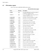
Страница 154: ...ETM ETMISEQ Output Sequential instruction access for the ETM ETMITBIT Output Thumb state indication for the ETM ETMDA 31 0 Output Data address for the ETM ETMDMAS 1 0 Output Data size indication for the ETM ETMDMORE Output More sequential data indication for the ETM ETMDnMREQ Output Data memory request for the ETM ETMDnRW Output Data not read or write for the ETM ETMDSEQ Output Sequential data ind...

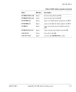
Страница 155: ...put Coprocessor handshake decode signals for the ETM ETMCHSE 1 0 Output Coprocessor handshake execute signals for the ETM ETMPASS Output Coprocessor instruction execute indication for the ETM ETMLATECANCEL Output Coprocessor late cancel indication for the ETM ETMPROCID Output Process ID for the ETM ETMPROCIDWR Output Asserted when ETMPROCID is written Table A 6 ETM interface signals continued Name...

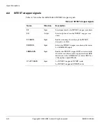
Страница 156: ...tput Serial output data from the INTEST wrapper scan chain SCANEN Input Enables scanning of data through the INTEST wrapper scan chain TESTEN Input Selects the INTEST wrapper scan chain as the source for ARM966E S inputs SERIALEN Input Enables the INTEST wrapper BIST activation mode where the scan chain is used to apply serialized ARM instructions to the ARM966E S to activate BIST test of the tigh...

Страница 157: ...ite DMAMAS 1 0 Input DMA Memory Access Size Encodes the size of writes Reads are always word wide 00 byte 01 halfword 10 word 11 reserved DMAD 31 0 Input DMA write data DMAWait Input DMA Wait Used to stall the ARM966E S to allow a DMA access to take place This functionality is only required if the data RAM is single port This signal must be tied LOW if the data RAM is dual port This signal has the...

Страница 158: ...Signal Descriptions A 16 Copyright 2000 ARM Limited All rights reserved ARM DDI 0186A ...

Страница 159: ...M Limited All rights reserved B 1 Appendix B AC Parameters This appendix describes the AC timing parameters for the ARM966E S It contains the following sections Timing diagrams on page B 2 AC timing parameter definitions on page B 12 ...

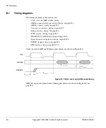
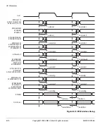
Страница 160: ...oprocessor interface timing on page B 5 Debug interface timing on page B 6 JTAG interface timing on page B 7 DBGSDOUT to DBGTDO timing on page B 8 Exception and configuration timing on page B 8 INTEST wrapper timing on page B 9 ETM interface timing on page B 10 Clock reset and AHB enable timing parameters are shown in Figure B 1 Figure B 1 Clock reset and AHB enable timing AHB bus request and gran...

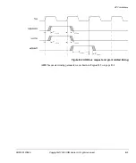
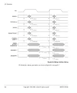
Страница 161: ...ACParameters ARM DDI 0186A Copyright 2000 ARM Limited All rights reserved B 3 Figure B 2 AHB bus request and grant related timing AHB bus master timing parameters are shown in Figure B 3 on page B 4 ...

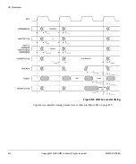
Страница 162: ...AC Parameters B 4 Copyright 2000 ARM Limited All rights reserved ARM DDI 0186A Figure B 3 AHB bus master timing Coprocessor interface timing parameters are shown in Figure B 4 on page B 5 ...

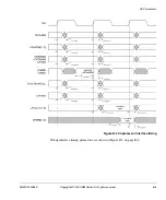
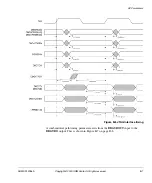
Страница 163: ...ACParameters ARM DDI 0186A Copyright 2000 ARM Limited All rights reserved B 5 Figure B 4 Coprocessor interface timing Debug interface timing parameters are shown in Figure B 5 on page B 6 ...

Страница 164: ...AC Parameters B 6 Copyright 2000 ARM Limited All rights reserved ARM DDI 0186A Figure B 5 Debug interface timing JTAG interface timing parameters are shown in Figure B 6 on page B 7 ...

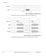
Страница 165: ...I 0186A Copyright 2000 ARM Limited All rights reserved B 7 Figure B 6 JTAG interface timing A combinatorial path timing parameter exists from the DBGSDOUT input to the DBGTDO output This is shown in Figure B 7 on page B 8 ...

Страница 166: ...ghts reserved ARM DDI 0186A Figure B 7 DBGSDOUT to DBGTDO timing Exception and configuration timing parameters are shown in Figure B 8 Figure B 8 Exception and configuration timing The INTEST wrapper timing parameters are shown in Figure B 9 on page B 9 ...

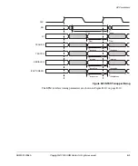
Страница 167: ...ved B 9 Figure B 9 INTEST wrapper timing The ETM interface timing parameters are shown in Figure B 10 on page B 10 CLK SO SI SCANEN TESTEN SERIALEN ICAPTUREEN Tihcaptureen Tiscapturee Tihserialen Tihtesten Tihscanen Tihsi Tissi Tohso Tovso Tisscanen Tistesten Tisserialen ...

Страница 168: ... 31 0 ETMWDATA 31 0 ETMMAS 31 0 ETMnWAIT ETMDMORE ETMDnMREQ ETMDnRW ETMDABORT ETMCHSD 1 0 ETMPASS ATMPLATECANCEL ETMDBGACK ATMRNGOUT 1 0 ETMEN FIFOFULL ETMBIGEND ETMHIVECS ETMPROCID ATMPRODCDWR Tovtminst Tohetminst Tovetmdata Tohetmdata Tovetmstat Tohetmstat Tovtmicti Tohetmiuctl Tovetmnwait Tohetmnwait Tovetmdctl Tohetmdctl Tovetmcfg Tohetmcfg Tovetmcpif Tohetmcpif Tovetmdbg Tohetmdbg Tihetmfiful...

Страница 169: ...ight 2000 ARM Limited All rights reserved B 11 The DMA interface timing parameters are shown in Figure B 11 Figure B 11 DMA interface timing CLK DMAReady DMARData DMAENABLE DMAnREQ DMAA DMAMAS DMAD DMAWait Tovdma Tohdma Tisdma Tihdma ...

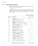
Страница 170: ...Min Max Tcyc CLK cycle time 100 Tishen HCLKEN input setup time to rising CLK 85 Tihhen HCLKEN input hold time from rising CLK 0 Tisrst HRESETn deassertion input setup time to rising CLK 90 Tihrst HRESETn deassertion input hold time from rising CLK 0 Tovreq Rising CLK to HBUSREQ valid 30 Tohreq HBUSREQ hold time from rising CLK 0 Tovlck Rising CLK to HLOCK valid 30 Tohlck HLOCK hold time from risin...

Страница 171: ...cpid Rising CLK to CPINSTR 31 0 valid 30 Tohcpid CPINSTR 31 0 hold time from rising CLK 0 Tovcpctl Rising CLK to transaction control valid 30 Tohcpctl Transaction control hold time from rising CLK 0 Tiscphs Coprocessor handshake input setup time to rising CLK 50 Tihcphs Coprocessor handshake input hold time from rising CLK 0 Tovcplc Rising CLK to CPLATECANCEL valid 30 Tohcplc CPLATECANCEL hold tim...

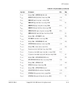
Страница 172: ...uts hold time from rising CLK 0 Tisdbgin Debug inputs setup time to rising CLK 30 Tihdbgin Debug inputs hold time from rising CLK 0 Tisiebkpt DBGIEBKPT input setup time to rising CLK 20 Tihiebkpt DBGIEBKPT input hold time from rising CLK 0 Tisdewpt DBGDEWPT input setup time to rising CLK 20 Tihdewpt DBGDEWPT input hold time from rising CLK 0 Tovdbgsm Rising CLK to debug state valid 30 Tohdbgsm Deb...

Страница 173: ...30 Tdsh DBGTDO hold time from DBGSDOUTBS changing 0 Tovbigend Rising CLK to BIGENDOUT valid 30 Tohbigend BIGENDOUT hold time from rising CLK 0 Tisint Interrupt input setup time to rising CLK 15 Tihint Interrupt input hold time from rising CLK 0 Tishivecs VINITHI input setup time to rising CLK 95 Tihhivecs VINITHI input hold time from rising CLK 0 Tisinitram INITRAM input setup time to rising CLK 9...

Страница 174: ...d time from rising CLK 0 Tovetmstat Rising CLK to ETMINSTREXEC valid 30 Tohetmstat ETMINSTREXEC hold time from rising CLK 0 Tovetmdata Rising CLK to ETM data interface valid 30 Tohetmdata ETM data interface hold time from rising CLK 0 Tovetmnwait Rising CLK to ETMnWAIT valid 30 Tohetmnwait ETMnWAIT hold time from rising CLK 0 Tovetmdctl Rising CLK to ETM data control valid 30 Tohetmdctl ETM data c...

Страница 175: ...st related and expected to operate at typically 50 of the functional clock rate Tisetmen ETMEN input setup time to rising CLK 50 Tihetmen ETMEN input hold time from rising CLK 0 Tisfifofull FIFOFULL input setup time to rising CLK 50 Tihetmen FIFOFULL input hold time from rising CLK 0 Tovdma Rising CLK to DMA signals valid 50 Tohdma DMA signals hold time from rising CLK 0 Tisdma DMA input setup tim...

Страница 176: ...AC Parameters B 18 Copyright 2000 ARM Limited All rights reserved ARM DDI 0186A ...

Страница 177: ...C SRAM Stall Cycles This appendix describes the tightly coupled SRAM in the ARM966E S It contains the following section About SRAM stall cycles on page C 2 For details of the ARM9E S interface signals referenced in this section refer to the ARM9E S Technical Reference Manual ...

Страница 178: ...e of write data from the ARM9E S core The write data appears on the core interface in the cycle after the address so that it is not possible to perform the write until the next rising clock edge The address from the core must therefore be pipelined to line up with the write data A write with pipelined address is shown in Figure C 1 Figure C 1 SRAM write cycle Note The write is performed on the sec...

Страница 179: ... a stall must occur before the read of Addr B C 1 2 Additional Instruction SRAM stalls The I SRAM has additional stall cycles that arise because of the following operations data reads to the I SRAM are pipeline simultaneous instruction fetches and data accesses can occur any access can occur during two cycle data reads and writes Simultaneous instruction fetch data read The ARM9E S data interface ...

Страница 180: ...quests from the ARM9E S core the instruction fetch is always performed first followed by the data read The core is disabled until both accesses have completed Data read To maximize the I SRAM interface frequency performance data read requests to this RAM are pipelined This adds a stall cycle for every data read instruction An example of a data read from the I SRAM is shown in on page C 5 Addr B I ...

Страница 181: ...irst read of the LDM Back to back LDRs will incur a stall cycle at the start of each LDR Data read followed by instruction fetch Data reads to the I SRAM are pipelined An instruction fetch in the cycle after a data read request coincides with the stalled data read and so the instruction fetch is stalled for 1 cycle This is shown in on page C 6 CLK DnMREQ DnRW DA 31 0 SRAM Addr RDATA 31 0 SYSCLKEN ...

Страница 182: ...uction fetch that both map to I SRAM address space two stall cycles occur The first cycle allows for the pipelined write the second cycle allows for the instruction fetch The core cannot be enabled until both accesses have completed see Figure C 6 on page C 7 CLK DnMREQ InMREQ DnRW DA 31 0 IA 31 0 I SRAM Addr RDATA 31 0 INSTR 31 0 SYSCLKEN Addr A read Addr A Addr B fetch Addr B Readdata A Readdata...

Страница 183: ... the next cycle It is similar to the generic read follows write scenario of each SRAM except that the read is an instruction fetch rather than a data load The instruction fetch must be held off until the write has completed requiring that the ARM9E S core is stalled for a cycle see Figure C 7 on page C 8 Addr B I fetch Read Instr B Write data A Addr A write CLK DnMREQ InMREQ DA 31 1 I SRAM Addr WD...

Страница 184: ... by both an instruction fetch and a data write The second write is performed immediately after the current write without penalty However the core must be stalled until both the second write and instruction fetch have completed so there are two stall cycles see Figure C 8 on page C 9 Addr B I fetch Read Instr B Write data A Addr A write CLK DnMREQ DA 31 1 I SRAM Addr WDATA 31 0 SYSCLKEN I SRAM writ...

Страница 185: ...is has the same two stall cycle response as the previous scenario although the I SRAM control behaves differently The first write must complete before the data read can be performed The instruction fetch can then be performed in the next cycle see Figure C 9 on page C 10 Addr A write CLK DnMREQ DnRW DA 31 1 I SRAM write cycle Addr B write stall cycle SRAM read cycle Read instr C Write data A Addr ...

Страница 186: ...ARM DDI 0186A Figure C 9 I SRAM write followed by instruction fetch data read Addr B I fetch Read Instr B Read data A Addr A read CLK DnMREQ InMREQ DA 31 1 I SRAM Addr RDATA 31 0 SYSCLKEN stall cycle Addr B INSTR 31 0 I SRAM inst fetch DnRW IA 31 1 Addr A I SRAM data read ...

Страница 187: ...erable write address space 3 4 Busy wait 7 5 abandoned 7 12 interrupted 7 12 C CHSDE A 6 CHSEX A 6 CLK A 3 Clock domains 8 14 interface signals A 3 system 8 3 test 8 3 COMMRX A 8 COMMTX A 9 Control register 2 5 Conventions typographical xiii Coprocessor handshake signals 7 5 handshake states 7 5 instruction busy wait 7 5 interface signals A 6 Core control register 2 7 Core state determining 8 15 C...

Страница 188: ... DMAD A 15 DMAENABLE A 15 DMAMAS A 15 DMAnREQ A 15 DMAnRW A 15 DMARData A 15 DMAReady A 15 DMAWait A 15 Drain write buffer 2 8 D SRAM 3 3 E EDBGRQ 8 18 A 9 EmbeddedICE RT 8 5 8 13 debug communications channel 8 19 debug status register 8 15 disabling 8 18 macrocell 8 16 operation 8 16 overview 8 16 Endian bit 2 7 ETM interface signals A 12 ETMBIGEND A 12 ETMCHSD A 13 ETMCHSE A 13 ETMDA A 12 ETMDAB...

Страница 189: ...CPINSTR A 6 CPLATECANCEL A 6 CPPASS A 6 CPTBIT A 7 DAMReady A 15 DBGACK 8 9 8 18 A 9 DBGDEWPT 8 18 A 10 DBGEN 8 18 A 9 DBGEXT A 9 DBGIEBKPT 8 18 A 10 DBGINSTREXEC A 9 DBGIR A 8 DBGnTDOEN A 8 DBGnTRST A 8 DBGRNG A 9 DBGRQ A 9 DBGSCREG A 8 DBGSDIN A 8 DBGSDOUT A 8 DBGTAPSM A 8 DBGTCKEN 8 14 A 3 DBGTDI A 8 DBGTDO A 8 DBGTMS A 8 DMAA A 15 DMAD A 15 DMAENABLE A 15 DMAMAS A 15 DMAnREQ A 15 DMAnRW A 15 D...

Страница 190: ...2 SRAM stall cycles 4 3 SRAM wrapper 4 7 Standby mode 2 8 States TAP controller 8 2 State debug 8 2 SYSCLKEN 8 14 System state determining 8 15 T TAP controller 8 5 8 16 states 8 2 TAPID A 10 TBIT 2 6 TCK 8 3 Test clock 8 3 register 2 9 Test Access Port 8 2 TESTEN A 14 Thumb instruction set 1 2 Typographical conventions xiii V VINITHI A 11 W Wait for interrupt 2 8 Watchpoints 8 11 8 16 8 17 except...

Отзывы: