


1161 Ringwood Ct, #110, San Jose, CA 95131, U. S. A. Tel.: (408) 748-9100, Fax: (408) 770-9187 www.analogtechnologies.com
Copyrights 2000-2021, Analog Technologies, Inc. All Rights Reserved. Updated on 3/11/2021
Email: [email protected]/[email protected] 2
Analog Technologies
ATLS1A102
Low Noise Constant Current Laser Driver
APPLICATIONS
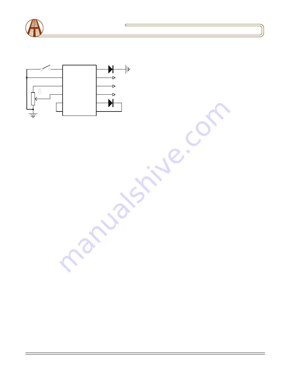
Figure 3 shows a stand-alone application circuit.
power supply 0V
D2
LED
3
1
2
W1
100K
(Clock-wise)
Power Supply 5V
S1
SPST
D1
Laser Diode
Shut Down
Loop Good Indication
(Optional)
LISH
6
LPGD
12
VPS
10
LDC
7
PGND
9
GND
2
P5V
5
SYNC
11
LDA
8
2P5V
3
LISL
4
SDN
1
ATLS1A102
Sync. Signal
Current Setting
Figure 3. A Typical Stand-alone Application Schematic
Output Noise
Since the controller uses a switch mode driver, there will be
some ripple noise at the switching frequency, 1MHz. The
voltage magnitude is about 30mV at this frequency.
For applications which cannot tolerate this noise, users can
choosing the same controller with the switch mode driver
disabled. The part number becomes ADLS1A102-D-L or
ADLS1A102-S-L.
The disadvantage to turn off the switch mode driver is that
the efficiency of the controller will be lowered, thus, the
controller’s temperature may rise to too high a value. The
power consumption of the controller will be calculated in
this way:
P
DRIVER
= I
OUT
× (V
VPS
– V
LDA
),
where I
OUT
is the output current;
V
VPS
is the power supply voltage;
V
DRIVER
is the voltage across the laser diode.
If the P
DRIVER
is >2W, heat sink might be needed.
When prefer not to use the heat sink, this is option: lowering
the controller power consumption by reducing the power
supply voltage VPS. Please make sure:
V
VPS
≥
V
DRIVERMAX
+ 1.2V,
where V
DRIVERMAX
is the maximum possible laser diode
voltage.
Turning the Controller On and Off
The controller can be turned on and off by setting the SDN
pin high and lower respectively. It is recommended to turn
the controller on by this sequence:
To turn on: turn on the power by providing the power supply
voltage to the controller, turn on the controller by releasing
the SDN pin.
To turn off: turn off the controller by lowering the voltage of
SDN pin, turn off the power by stopping the voltage supply on
the VPS pin.
When not controlling by the SDN pin: leave it unconnected and
turn on and off the controller by the power supply.
In Figure 3, S1 is the shut down switch. The internal equivalent
input circuit of SDN pin is a pull-up resistor of 100k being
connected to VPS. If not using a switch (S1) to control the
laser, leave the SDN pin unconnected. D1 is the laser diode,
which is float from the ground and the VPS, with its anode
connected to the LDA, pin 8, and cathode connected to the
LDC, pin 7. D2 is an LED, indicating when the control loop
works properly, that is: the output current equals to the input
set value. This pin has an internal pull up resistor of 5k to the
power supply pin, VPS, pin 10. The pull down resistance is
200
Ω
. When higher pull up current is needed for such as
driving an LED, an external resistor can be placed between the
VPS and the LPGD pins. Make sure that the resistor is not too
small that the pull down resistor will not be able to pull the pin
low enough when the controller loop is not good. When
choosing not to use an LED for indicating the working status,
leave the LPGD pin unconnected.
Setting the Output Current
The LPGD pin can also be connected to a digital input pin of a
micro-controller, when software/firmware is utilized in the
system.
The output current is set by adjusting W1, which sets input
voltages of LISL, pin 4. The output current will be:
I
OUT
(A) = V
LISL
(V)/2.5 (V).
LISL should never be left float. Otherwise, the output current
will go too high a value that the laser might be damaged.
The LISL pin allows modulating the output current at a speed
of up to 0.08Hz. This low speed port filters out high frequency
noise, if any, in the input signal applied to this pin.
In addition to using the LPGD pin for monitoring the working
status of the controller, the output current can be monitored
directly by measuring the voltage of LIS pin when LPGD (loop
good) pin is high,. The equation is:
I
OUT
(A) = V
LIS
(V)/2.5 (V)
For example, when seeing LIS = 2.5V, the output current is
2.5V/2.5V = 1A.
Figure 4 shows an application where ATLS1A102 is interfaced
with a micro-controller.
LIO
ADC
10K


