


Preliminary Technical Data
EVAL-AD5934EB
Rev. PrC | Page 21 of 32
Measuring Small Impedances
The AD5934 is capable of measuring impedance values of up to
10 MΩ if the system gain settings are chosen correctly for the
impedance subrange of interest. However, there are two points
to understand when measuring small impedances with the
AD5934.
First, if the user places a small impedance value (< ≈ 500 Ω over
the sweep frequency of interest) between the VOUT and VIN
pins, the signal current flowing through the impedance for a
fixed excitation voltage increases in accordance with Ohm’s law.
The output stage of the transmit side amplifier that is available
at the VOUT pin may not be able to provide the required
increase in current through the impedance. In addition, to
ensure a unity gain condition on the receive side I-V amplifier,
there must be a similar small value of feedback resistance for
system calibration, as outlined in the Calibrating the AD5934
section. The voltage presented at the VIN pin is hard biased at
VDD/2 due to the virtual earth on the receive side I-V amplifier
(see the
data sheet for further details). The increased
current’s sink/source requirement on the output of the receive
side I-V amplifier may also cause the amplifier to operate
outside of the linear region, resulting in significant errors in
subsequent impedance measurements.
Second, the value of the output series resistance (R
OUT
see
Figure 28 ) at the VOUT pin of the AD5934 must be taken into
account when measuring small impedances (Z
UNKNOWN
),
specifically when the value of the output series resistance is
comparable to the value of the impedance being tested
(Z
UNKNOWN
). If the R
OUT
value is unaccounted for in the system
calibration (that is, the gain factor calculation) when measuring
small impedances, an error will be introduced in subsequent
impedance measurements. (The error introduced depends on
the relative magnitude of the impedance being tested compared
with the value of the output series resistance.)
The value of the output series resistance depends on the
selected output excitation range at VOUT, and, like with all
discrete resistors manufactured in a silicon fabrication process,
the tolerance varies from device to device. Typical values of the
output series resistance are listed in Table 6.
Table 6. Output Series Resistance (R
OUT
) vs. Excitation Range
Parameter Value
(Typ)
Output Series
Resistance Value (Typ)
Range 1
2 V p-p
200 Ω
Range 2
1 V p-p
2.4 kΩ
Range 3
0.4 V p-p
1.0 kΩ
Range 4
0.2 V p-p
600 Ω
Therefore, to accurately calibrate the AD5934 to measure small
impedances, it is necessary to reduce the signal current by
sufficiently attenuating the excitation voltage and to account for
the output series resistance value (R
OUT
) by factoring it into the
gain factor calculation (see the
details).
During device characterization, measuring the output series
resistance value (R
OUT
) was achieved by selecting the appropriate
output excitation range at VOUT and then sinking and sourcing
a known current (for example, ±2 mA) at the pin and measuring
the change in dc voltage. The output series resistance was cal-
culated by measuring the inverse of the slope (that is, 1/slope)
of the resultant I-V plot.
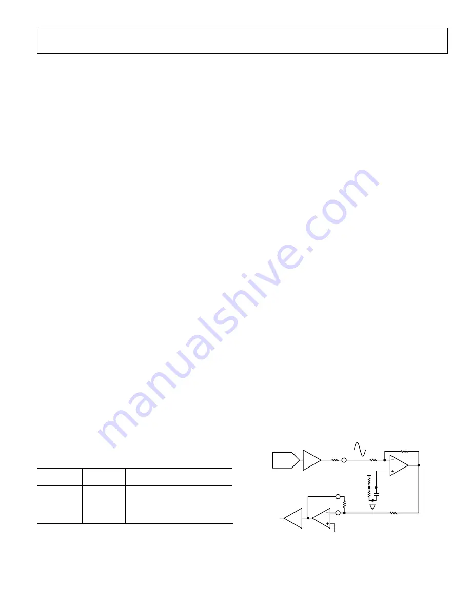
A circuit that helps to minimize the effects of the two previously
described issues is shown in Figure 28. The aim of this circuit is
to place the AD5934 system gain within its linear range when
measuring small impedances by using an additional external
amplifier circuit along the signal path. The external amplifier
attenuates the peak-to-peak excitation voltage at VOUT if the
user chooses suitable values for Resistors R1 and R2. This
reduces the signal current flowing through the impedance and
minimizing the effect of the output series resistance in the
impedance calculations.
In the circuit shown in Figure 28, the impedance being tested
(Z
UNKNOWN
) sees the output series resistance of the external
amplifier. This value is typically much less than 1 Ω with
feedback applied, depending on the op amp device (for
example, AD820, AD8641, or AD8531), the load current, the
bandwidth, and the gain.
The key point is that the output impedance of the external
amplifier in Figure 28, which is also in series with the
impedance being tested (Z
UNKNOWN
), has a far less significant
effect on the AD5934 calibration (that is, the gain factor
calculation) and subsequent impedance readings in comparison
with those obtained by connecting the small impedance directly
to the VOUT pin (and directly in series with R
OUT
). The
external amplifier buffers the unknown impedance from the
effects of the output series resistance of the AD5934 (R
OUT
) and
introduces a smaller output impedance in series with the
impedance being tested (Z
UNKNOWN
).
05
44
9
-02
8
R
OUT
V
OUT
AD8531
AD820
AD8641
AD8627
V
DD
V
DD
/2
1µF
20k
Ω
20k
Ω
Z
UNKNOWN
R
FB
R
FB
V
IN
V
DD
/2
PGA
I-V
R2
R1
DDS
TRANSMIT SIDE
OUTPUT AMPLIFIER
2V p-p
Figure 28. Additional External Amplifier Circuit
for Measuring Small Impedances