background image

EVAL-AD5676SDZ/EVAL-AD5676RSDZ User Guide 

UG-814 


Rev. A | Page 5 of 12 

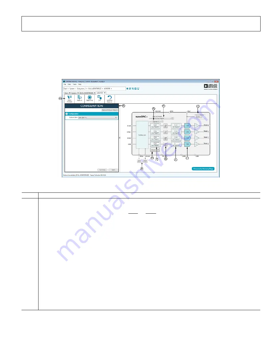
BLOCK DIAGRAM AND DESCRIPTION 

The 

EVAL-AD5676SDZ

/

EVAL-AD5676RSDZ

 software is 

organized so that it appears similar to the functional block 
diagram shown in the data sheets. In this way, it is easy to 
correlate the functions on the board with the description in the 
data sheets. A full description of each block, register, and its 
settings is given in the 

AD5676

/

AD5676R

 data sheets. 

Some of the blocks and their functions are described here as 
they pertain to the evaluation board. The full screen block 
diagram is shown in Figure 4 and Table 1 describe the 
functionality of each block. 

12993-

004


Figure 4. Block Diagram with Labels 

Table 1. Block Diagram Functions 

Label 

Function 

The configuration wizard sets up the initial configuration for the board. From the Output Gain drop-down menu, the reference 
gain case be selected. A gain of 1 is the default. After setting up the initial configuration, click Apply and the values are applied. 
These settings can be modified at any stage while testing. 

The GPIO buttons act as external GPIO pulses to the LDAC and RESET pins. The LDAC button pushes data from both input 
registers (E) to the DAC registers (F). The RESET button clears all data from input registers and DAC registers. These buttons are 
live, so there is no need to click Apply Changes (K). 

The Command Option drop-down menu selects how the data being transferred to the device affects the Input and DAC registers. 

After a data value is entered in an input register (see E), this menu determines if the data is transferred to the input register only, or 
to the channel input register (E) and channel DAC register (F).  

The Change Page Display drop-down menu selects which page of 4 DAC channel settings are displayed 

The input registers transfer 16-bit data word to the device. Upon clicking the Apply Changes (K), this 16-bit data word is 
transferred to the device.  

The DAC registers display the value that is currently present in the DAC register on the device. The DAC registers can be updated 
by selecting the appropriate command option or by toggling LDAC (B). 

Software reset returns the board and software to default values. This button is live, so there is no need to click Apply Changes

The Load LDAC buttons per channel control to control the loading of Input Register contents to the DAC Register. 

The DAC Configuration options provide access to per channel configuration options such as power-down options and hardware 
LDAC mask setting. 

Selecting enabled from the internal reference setting enables the on-chip reference for the board, if disabled is selected, an 
external reference must be applied. This control is only available on th

AD5676R

The Apply Changes button applies all modified values to the device. Note that if an evaluation board is not connected, values 
entered into the Input Registers are not transferred to the DAC registers. 


Содержание EVAL-AD5676RSDZ

Страница 1: ... AD5676R octal channel voltage output digital to analog converter DAC The EVAL AD5676SDZ EVAL AD5676RSDZ evaluation boards help users to quickly prototype new AD5676 AD5676R circuits and reduce design time The AD5676 AD5676R operate from a single 2 7 V to 5 5 V supply The AD5676R has an internal 2 5 V reference giving a maximum output voltage of 2 5 V or 5 V The AD5676 does not have an internal re...

Страница 2: ...ns 8 Evaluation Board Circuitry 9 Evaluation Board Schematics 10 Bill of Materials 12 REVISION HISTORY 5 2017 Rev 0 to Rev A Changes to Features Section Additional Equipment and Software Needed Section Online Resources Section and General Description Section 1 Changes to Installing the Software Section Changed Evaluation Board Setup Procedures Section to Initial Set Up Section 4 Added Figure 3 and...

Страница 3: ...EVAL AD5676SDZ EVAL AD5676RSDZ User Guide UG 814 Rev A Page 3 of 12 TYPICAL EVALUATION SETUP 12993 001 SDP BOARD AD5676R EVALUATION BOARD COM 25V 6V 6 000V 0 250A POWER SUPPLY CONNECTORS Figure 1 ...

Страница 4: ...llation is finished the EVAL AD5676SDZ and EVAL AD5676RSDZ evaluation board plug ins appear when you open ACE INITIAL SETUP To set up the evaluation board take the following steps 1 Connect the evaluation board to the SDP B board and connect the USB cable between the SDP B board and the PC 2 Power the SDP B and evaluation board by connecting 6 V dc to the J3 connector 3 Run the ACE application The...

Страница 5: ...e Command Option drop down menu selects how the data being transferred to the device affects the Input and DAC registers After a data value is entered in an input register see E this menu determines if the data is transferred to the input register only or to the channel input register E and channel DAC register F D The Change Page Display drop down menu selects which page of 4 DAC channel settings...

Страница 6: ...e toggled Apply Changes is used to transfer data to the device All changes here correspond to the block diagram for example if the internal register bit is enabled it shows as enabled on the block diagram Any bits or registers that are in bold are modified values that have not been transferred to the board After Apply Changes is clicked the data is transferred to the board 12993 005 Figure 5 AD567...

Страница 7: ... to avoid ground loop problems All supplies are decoupled to ground with 10 μF tantalum and 0 1 μF ceramic capacitors Table 2 Power Supply Connectors Connector Number Voltage J1 External VLOGIC supply J2 Analog power supply VCC J3 6 V dc board positive power supply INPUT SIGNALS When the SDP B board is used to control the evaluation board the digital input signals are applied to Connector J4 When ...

Страница 8: ...oltage source A Position A selects the internal voltage source INT_VCC from the ADP3331 U1 Position B selects an external supply voltage EXT_ VCC LK2 This link selects the DAC digital voltage source A Position A selects the digital voltage source from the SDP B board V_IO Position B selects an external digital supply voltage EXT_VLOGIC LK3 This link selects the reference source A B1 Position A sel...

Страница 9: ...or J3 Alternatively a separate analog supply can be attached via Connector J2 and an external VLOGIC supply can be connected to Connector J1 Control of the AD5676 AD5676R is typically performed by the SDP B board which is attached to Connector J4 The SDP B board allows the software provided with the kit to be used to load register values set the voltage of the DAC outputs and write to the control ...

Страница 10: ...UG 814 EVAL AD5676SDZ EVAL AD5676RSDZ User Guide Rev A Page 10 of 12 EVALUATION BOARD SCHEMATICS 12993 006 Figure 8 EVAL AD5676SDZ EVAL AD5676RSDZ Schematic Page 1 of 2 ...

Страница 11: ...EVAL AD5676SDZ EVAL AD5676RSDZ User Guide UG 814 Rev A Page 11 of 12 12993 007 Figure 9 EVAL AD5676SDZ EVAL AD5676RSDZ Schematic Page 2 of 2 ...

Страница 12: ...s expressly made subject to the following additional limitations Customer shall not i rent lease display sell transfer assign sublicense or distribute the Evaluation Board and ii permit any Third Party to access the Evaluation Board As used herein the term Third Party includes any entity other than ADI Customer their employees affiliates and in house consultants The Evaluation Board is NOT sold to...

Отзывы: