background image

UG-976 

EVAL-AD5325DBZ User Guide 


Rev. A | Page 4 of 13 

EVALUATION BOARD SOFTWARE QUICK START PROCEDURES 

INSTALLING THE SOFTWARE 

The 

AD5325

 evaluation software is compatible with Windows® 

Vista (64-bit/32-bit) and Windows 7 (64-bit/32-bit). 
Install the software before connecting the 

SDP-B

 board to the 

USB port of the PC to ensure that the 

SDP-B

 board is 

recognized when it connects to the PC. 
To install the 

AD5325

 evaluation software, take the following 

steps: 
1.


Start the Windows operating system. 

2.


Download the installation software from the 

EVAL-

AD5325DBZ

 evaluation board page. 

3.


Run the 

setup.exe

 file from the installer folder if it does not 

open automatically. 

4.


After the installation is complete, power up the evaluation 
board as described in the Power Supplies section. 

5.


Connect the 

EVAL-AD5325DBZ

 evaluation board to the 

SDP-B

 controller board and connect the 

SDP-B

 board to 

the PC using the USB cable included in the evaluation kit. 

6.


When the software detects the 

EVAL-AD5325DBZ

proceed through any dialog boxes that appear to finalize 
the installation. 

RUNNING THE SOFTWARE 

To run the program, do the following: 
1.


Connect the evaluation board to the 

SDP-B

 board and 

connect the USB cable between the 

SDP-B

 board and the PC. 

2.


Power up the evaluation board as described in the Power 
Supplies section. 

3.


From the 

Start

 menu, click 

All Programs

Analog Devices

AD5325 Evaluation Software

If the 

SDP-B

 board is not connected to the USB port when the 

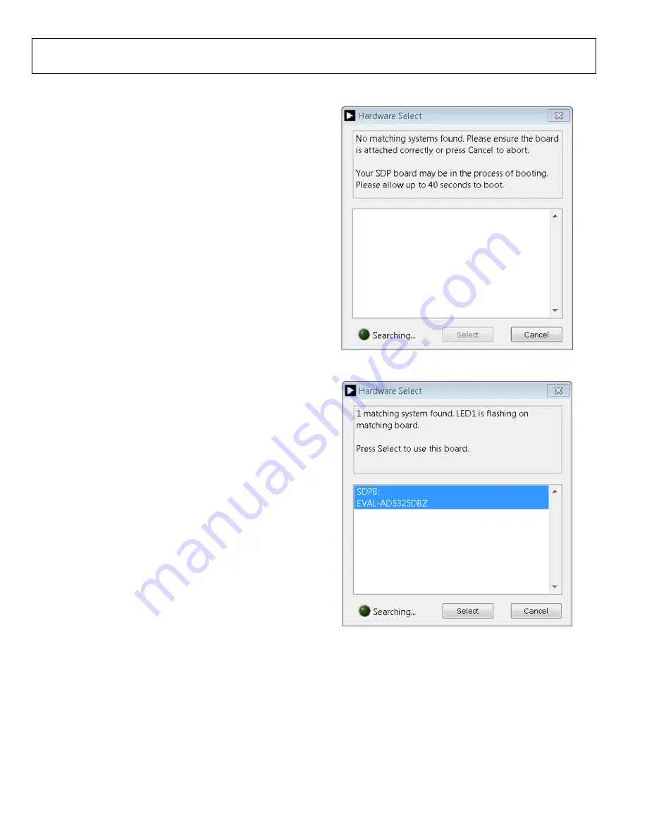
software is launched, a connectivity error displays (see Figure 2). 
Connect the evaluation board to the USB port of the PC and 
wait a few seconds. When the 

SDP-B

 board is detected, the 

display is updated (see Figure 3). 
Alternatively, the software can be used without an evaluation 
board. The software runs in simulation mode displaying 
expected outputs based on the input data. The main window of the 

AD5325

 evaluation software then opens, as shown in Figure 4. 

14455-

002


Figure 2. Connectivity Error 

14455-

003


Figure 3. Hardware Select 


Содержание EVAL-AD5325DBZ

Страница 1: ...REQUIRED EVAL SDP CB1Z board SDP B controller board must be purchased separately GENERAL DESCRIPTION This user guide details the operation of the evaluation board for the AD5325 quad channel voltage output DAC The evaluation board is designed to help users quickly prototype new AD5325 circuits and reduce design time The AD5325 operates from a single 2 5 V to 5 5 V supply Full details are available...

Страница 2: ...Hardware 3 Power Supplies 3 Motherboard Link Options 3 Daughter Board Link Options 3 Evaluation Board Software Quick Start Procedures 4 Installing the Software 4 Running the Software 4 Software Operation 5 Evaluation Board Schematics and Artwork 6 EVAL MBnanoDAC SDZ Motherboard 6 EVAL AD5325DBZ Daughter Board 10 Ordering Information 12 Bill of Materials 12 REVISION HISTORY 10 2017 Rev 0 to Rev A C...

Страница 3: ...ble 2 and Table 4 match the evaluation board imprints see Figure 11 Table 2 Link Options Setup for SDP B Control Default Link Number Position REF1 2 5V REF2 EXT REF3 EXT REF4 EXT LK5 C LK6 3 3V LK7 B DAUGHTER BOARD LINK OPTIONS The EVAL AD5325DBZ daughter board has one link option This link sets the least significant bit LSB of the I2 C address of the DAC Table 3 describes the function of the link...

Страница 4: ... using the USB cable included in the evaluation kit 6 When the software detects the EVAL AD5325DBZ proceed through any dialog boxes that appear to finalize the installation RUNNING THE SOFTWARE To run the program do the following 1 Connect the evaluation board to the SDP B board and connect the USB cable between the SDP B board and the PC 2 Power up the evaluation board as described in the Power S...

Страница 5: ...tively Power Down Control All of the DACs can be powered down simultaneously The DACs have a selection box that allows the device to operate in normal mode or in three different power down modes Click the blue progressive disclosure button on the POWER DOWN LOGIC block to access the Powerdown configuration window which allows the device to operate in normal mode or power down mode as shown in Figu...

Страница 6: ...PIO6 46 GND 45 GPIO4 44 GPIO2 43 GPIO0 42 SCL_1 41 SDA_1 40 GND 39 SPI_SEL1 SPI_SS 38 SPI_SEL_C 37 SPI_SEL_B 36 GND 35 SPORT_INT 34 SPI_D3 33 SPI_D2 32 SPORT_DT1 31 SPORT_DR1 30 SPORT1_TDV 29 SPORT0_TDV 28 GND 27 PAR_FS1 26 PAR_FS3 25 PAR_A1 24 PAR_A3 23 GND 22 PAR_CS 21 PAR_RD 20 PAR_D1 19 PAR_D3 18 PAR_D5 17 GND 16 PAR_D7 15 PAR_D9 14 PAR_D11 13 PAR_D13 12 PAR_D14 11 GND 10 PAR_D17 9 PAR_D19 8 P...

Страница 7: ...L LDAC CLR PD GAIN SDA 1 2 3 4 5 6 7 8 J9 J8 1 J8 2 J8 3 J8 4 J8 5 J8 6 J7 1 J7 2 J7 3 J7 4 J7 5 J7 6 J3 1 J3 2 J3 3 J3 4 J3 5 J3 6 J4 1 J4 2 J4 3 J4 4 J4 5 J4 6 J4 7 J4 8 VDD VREF1 VREF2 VREF3 VREF4 VLOGIC SDA SCL SYNC SCLK SDO SDIN LDAC CLR PD GAIN DB6 DB7 DB8 DB9 DB0 DB1 DB2 DB3 VOUT_0 VOUT_1 VOUT_2 VOUT_3 VOUT_4 VOUT_5 VOUT_6 VOUT_7 SCL SDA DGND VLOGIC SCL SDA DGND VLOGIC SYNC SDO SDIN SCLK DG...

Страница 8: ...UG 976 EVAL AD5325DBZ User Guide Rev A Page 8 of 13 14455 011 Figure 11 Motherboard Component Placement 14455 012 Figure 12 Motherboard Top Side Routing ...

Страница 9: ...EVAL AD5325DBZ User Guide UG 976 Rev A Page 9 of 13 14455 013 Figure 13 Motherboard Bottom Side Routing ...

Страница 10: ...J3 4 J3 5 J3 6 J4 1 J4 2 J4 3 J4 4 J4 5 J4 6 J4 7 J4 8 1 2 3 4 5 6 7 8 9 10 11 12 13 14 15 16 J1 A B LK1 VREF1 VDD SDA SCL VOUT_0 VOUT_1 VOUT_2 VOUT_3 VDD VDD VREF1 VREF2 VREF3 VREF4 VLOGIC SDA SCL SYNC SCLK SDO SDIN LDAC CLR PD GAIN VOUT_0 VOUT_1 VOUT_2 VOUT_3 VOUT_4 VOUT_5 VOUT_6 VOUT_7 DB6 DB7 DB8 DB9 DB0 DB1 DB2 DB3 DGND CS WR DB11 DB5 DB10 DB4 AGND 14455 014 Figure 14 Daughter Board Schematic...

Страница 11: ...EVAL AD5325DBZ User Guide UG 976 Rev A Page 11 of 13 14455 017 Figure 17 Daughter Board Bottom Side Routing ...

Страница 12: ...J10 120 way connector FEC 1324660 1 L1 Inductor SMD 600 Ω FEC 9526862 1 LK5 6 pin 3 2 0 1 inch header and shorting block FEC 148 535 and 150 411 36 pin strip 2 LK6 LK7 4 pin 2 2 0 1 inch header and shorting block FEC 148 535 and 150 411 36 pin strip 4 REF1 REF2 REF3 REF4 10 pin 5 2 0 1 inch header and shorting block FEC 1022227 and 150 411 1 R1 Resistor surge 1 6 Ω 1 0603 FEC 1627674 2 R2 R3 SMD r...

Страница 13: ...sublicense or distribute the Evaluation Board and ii permit any Third Party to access the Evaluation Board As used herein the term Third Party includes any entity other than ADI Customer their employees affiliates and in house consultants The Evaluation Board is NOT sold to Customer all rights not expressly granted herein including ownership of the Evaluation Board are reserved by ADI CONFIDENTIAL...

Отзывы: