background image

UG-1819 

EVAL-AD4114SDZ

 User Guide 


Rev. 0 | Page 16 of 24 

31

33

37

38

32

39

36

34

35

24002-

020


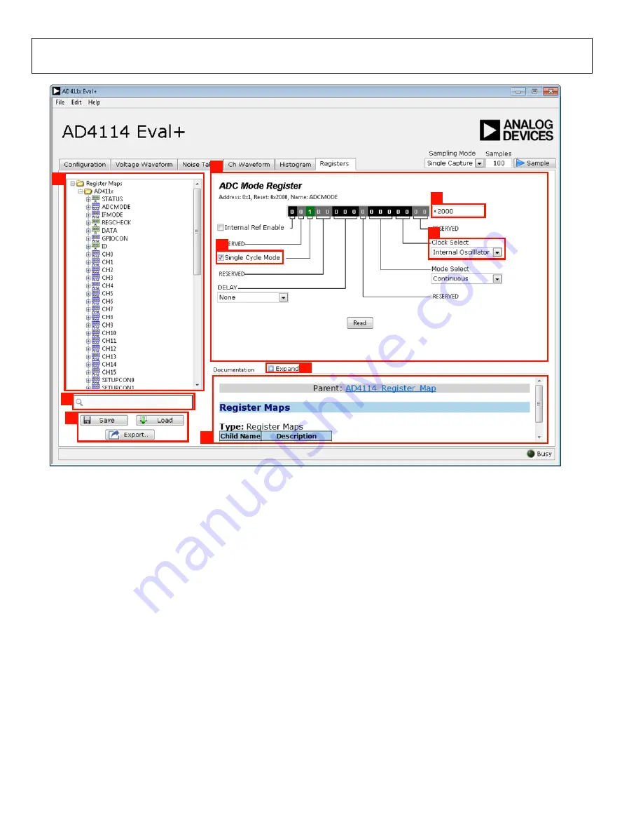
Figure 20. 

Registers

 Tab 

REGISTER MAP TAB (ADVANCED MODE ONLY) 

Register Maps List 

Click the Register Maps nested list (Label 31 in Figure 20) to 
show each register. Click the expand button next to each 

register to show the bit fields contained within that register.  

Register Maps Search 

The search box (Label 32 in Figure 20) allows the user to search 
the register maps list for any register or bit field. Entering a 

value into this control filters the register list.  

Register and Bit Field Control 

The register control area (Label 33 in Figure 20) allows the user to 
change the individual bit of the register selected in the register map 
list by clicking the bits in the register control or by programming 
the register value directly into the value control box (Label 34 in 
Figure 20). The register and bit controls also show all bit fields for 
the selected register. Change the values by using the Clock Select 
dropdown menu (Label 35 in Figure 20) or by selecting or clearing 

the Single Cycle Mode check box (Label 36 in Figure 20).  

Documentation 

The Documentation area (Label 38 in Figure 20) contains the 
documentation for the register or the bit field selected. This field 
can be updated by selecting a register or bit field in the register 
list, or by hovering over the register or bit field in the register 
list or register control. To display the Documentation area in a 

separate window click Expand (Label 37 in Figure 20). 

Save and Load 

Save and Load (Label 39 in Figure 20) allow the user to save the 
current register map setting to a file and to load the setting from 
the same file, respectively. The Export button exports the register 
settings as a header file that is compatible with th

AD411x no 

operating system software drivers

, which allows the user to 

quickly save their preferred configuration for prototyping use.  

EXITING THE SOFTWARE 

To exit the software, click the close button in the title bar. 

Содержание EVAL-AD4114

Страница 1: ...valuate all the features of the AD4114 The AD4114 is a 24 bit 31 25 kSPS Σ Δ analog to digital converter ADC with a 10 V input voltage range 16 single ended channels or eight fully differential channels All channels have on board overvoltage and overcurrent protection The EVAL AD4114SDZ includes voltage references and power and data insulation and can be connected to the Analog Devices Inc system ...

Страница 2: ...surement 4 Evaluation Board Hardware 5 Device Description 5 Hardware Link Options 5 Evaluation Board Setup Procedure 5 Serial Interface 6 Power Supplies 6 Analog Inputs 6 Reference Options 6 Evaluation Board Software 7 Software Installation Procedures 7 Software Operation 11 Configuration Tab 11 Waveform Tabs 13 Histogram Tab 15 Register Map Tab Advanced Mode Only 16 Exiting the Software 16 Evalua...

Страница 3: ...OWN POWER 5V OR 3 3V ADuM5411 POWER AND DATA POWER 5V OR 3 3V VOLTAGE INPUTS PROTECTION VIN0 VIN1 VIN2 VIN3 VIN4 VIN5 VIN6 VIN7 VINCOM XTAL AND INTERNAL CLOCK OSCILLATOR CIRCUITRY RAIL TO RAIL REFERENCE INPUT BUFFERS Σ Δ ADC 1 8V LDO MUX 1 8V LDO INT REF SERIAL INTERFACE DIGITAL FILTER BUFFERED PRECISION REFERENCE AD4114 TEMPERATURE SENSOR AVDD VIN8 VIN9 VIN10 VIN11 VIN12 VIN13 VIN14 VIN15 PRECISI...

Страница 4: ...o search for the SDP drivers Choose to automatically search for the drivers for the SDP board if prompted by the operating system 4 Launch the AD411x Eval software from the Analog Devices subfolder in the Programs menu QUICK START MEASUREMENT Use the following procedure to capture data quickly 1 Connect the dc signal source to a selected voltage input for example the VIN0 pin and VIN1 pin for diff...

Страница 5: ...e Arduino headers are used the J6 links must be changed to ARD 3 Ensure that LK3 is in Position B USB 4 Connect the SDP board to the PC using the USB cable Table 1 Default Link and Solder Link Options Link Default Option Description LK1 Inserted Connects the on board external reference ADR4525ARZ U2 to AD4114 U1 Remove LK1 if using a different single ended external reference LK2 Inserted Connects ...

Страница 6: ...Z includes an external 2 5 V reference the ADR4525ARZ By default LK1 is inserted connecting the external reference to the REF pin of the AD4114 Remove LK1 if using a different single ended external reference In the AD411x Eval evaluation software click the blue pop up button associated with Setup 0 to Setup 7 to select the reference used for conversions by the AD4114 see Figure 16 The pop up butto...

Страница 7: ...from the EVAL AD4114SDZ product page 2 Double click the setup exe file to begin the evaluation board software installation The software then installs to the following default location C Program Files x86 Analog Devices AD411x Eval 3 A dialog box appears asking for permission to allow the program to make changes to the PC Click Yes see Figure 3 24002 003 Figure 3 Granting Permission for the Program...

Страница 8: ...teps to install the SDP drivers 1 Click Next to proceed with the installation wizard 24002 008 Figure 8 Welcome Window for SDP Drivers Installations 2 With the SDP board still disconnected from the USB port of the PC ensure that all other applications are closed and then click Install 24002 009 Figure 9 Beginning the SDP Drivers Installation 3 To complete the driver installation click Close which ...

Страница 9: ... launch the AD411x Eval software as follows 1 From the Start menu click Programs Analog Devices AD411x Eval AD411x Eval exe The dialog box shown in Figure 13 appears Select AD4114 Evaluation Board and the main window of the software shown in Figure 16 appears 24002 013 Figure 13 AD4114 Evaluation Board Selection 2 If the EVAL AD4114SDZ is not connected to the USB port via the SDP when the software...

Страница 10: ...UG 1819 EVAL AD4114SDZ User Guide Rev 0 Page 10 of 24 9 8 1 2 3 4 11 7 12 10 13 5 6 24002 016 Figure 16 Configuration Tab in Quick Start Mode ...

Страница 11: ...shows the Configuration tab in detail and the following sections discuss the different elements on the Configuration tab of the software window Inputs Quick Start Mode Only The AD4114 has 16 voltage inputs which can be configured as single ended or fully differential pairs Label 1 in Figure 16 Use the Vin0 Vin7 and Vin8 V15 buttons to select between inputs The voltage range can also be set per inp...

Страница 12: ...n button on the block diagram opens the configuration window for that block Configuration Pop Up Button Each configuration button Label 7 in Figure 16 opens a different window to configure the relevant functional block External Parameters There are three external parameters that are set by the EVAL AD4114SDZ but must be entered into the software The three external parameters are the external refer...

Страница 13: ...of samples specified in the Samples box If Sampling Mode is set to Continuous the ADC continuously returns samples until stopped by the user Samples specifies the amount of samples to be shown on the data graph Samples is unrelated to the ADC mode Sample Click Sample Label 18 in Figure 18 to start gathering ADC results Results appear in the waveform graph Plot Selection The plot selection control ...

Страница 14: ...The Noise Analysis box shows the analysis of the input selected via the analysis control Label 22 in Figure 18 Noise Analysis The noise analysis area Label 23 in Figure 18 displays the results of the noise analysis for the selected analysis input including both noise and resolution measurements Input Range The Range box Label 24 in Figure 18 is an indicator in quick start mode The value is selecte...

Страница 15: ...oise Analysis The noise analysis area Label 27 in Figure 19 displays the results of the noise analysis for the selected analysis input including both noise and resolution measurements Display Units and Axis Controls Click the Units V mV A mA box in the Graph Configuration area Label 29 in Figure 19 to select whether the data graph displays in units of voltages amps or codes This control is indepen...

Страница 16: ...trols also show all bit fields for the selected register Change the values by using the Clock Select dropdown menu Label 35 in Figure 20 or by selecting or clearing the Single Cycle Mode check box Label 36 in Figure 20 Documentation The Documentation area Label 38 in Figure 20 contains the documentation for the register or the bit field selected This field can be updated by selecting a register or...

Страница 17: ... AD4114BCPZ GND_ISO 0 1UF DNI 0 1UF 1UF GND_ISO 0 1UF 1UF 1UF VIN4 GND_ISO CS_ISO SCLK_ISO GND_ISO 100K MOSI_ISO VINCOM VA_ISO VIN3 VIN10 DNI VIN15 VA_ISO VIN13 VIN2 VIN0 GND_ISO VIN14 0 VIN5 VIN6 GND_ISO VA_ISO DNI DNI VIN11 VA_ISO 16MEGHZ VIN7 VIN8 VIN9 VIN12 VIN1 IN IN IN IN IN IN IN IN IN IN IN IN OUT PAD REF REF GPIO3 VIN15 VIN14 VIN13 VIN12 VIN11 VIN10 VIN9 VIN8 VIN7 VIN6 VIN5 VIN4 GPIO2 GPI...

Страница 18: ...F GND_ISO D3 R17 4700PF DNI C34 180 180 C35 VIN3 VIN2 C25 D6 4700PF DNI VIN0 GND_ISO C27 GND_ISO 8 7 2 LK2 GND_ISO R24 D12 1 GND_ISO VIN15 C33 C30 VIN6 VIN7 VIN5 C31 VIN13 VIN1 VINCOM VIN14 VIN4 DNI VIN8 VIN9 C32 D10 180 C11 J3 5 4 3 GND_ISO GND_ISO GND_ISO GND_ISO C26 C24 C23 C22 C20 C19 D9 D8 D7 D5 D4 D2 D1 D16 D15 D13 D11 C18 C17 C16 C15 C14 C12 C29 C28 R16 R14 R15 R13 R12 R20 R23 R22 R25 9 8 7...

Страница 19: ...7 27 95 26 99 21 100 60 57 79 42 41 35 82 33 34 83 84 39 85 37 38 91 31 88 32 90 92 29 30 89 87 48 73 49 72 59 62 5 1 116 65 R42 U4 1 2 3 6 5 8 4 7 J8 1 2 3 4 5 6 J11 2 6 1 2 3 4 5 6 8 2 3 4 6 7 8 9 10 J10 1 3 5 6 1 2 3 2 D20 16 1 1 1 MISO 1 SCLK 1 5V 1 V_IO 1 C53 SDA_ARD SCLK_ARD_STD 7 V_IO R45 100K MOSI_SDP CS_SDP 1 3 V_IO_ARD 5 4 1 3 13 7 18 17 9 CS LK4 5 3 DNI J6 SCLK_ARD MISO_ARD SCLK_ARD V_U...

Страница 20: ...43 C41 C37 C36 R37 D18 C50 R39 C52 C51 3 2 1 LK3 3 2 1 J4 _MISO _MOSI _CS _SCLK R34 R33 R32 R31 R27 GND1 B1 B2 B3 B5 B6 B4 15 6 20 21 22 14 19 5 3 18 11 1 17 8 16 13 12 9 2 U3 SMAJ5 0A TR 1K V_USB MISO 0 1UF V_IO GND_ISO MOSI_ISO CS_ISO GND_ISO DNI DNI 10UF 33 1UF MOSI 33 GND_ADUM DNI 33 4 7NF GND_ISO 0 1UF 33 DNI 10UF GND_ISO VA_ISO SCLK_ISO 10UF SCLK V_SEL 14K 16 9K 10K 4 7NF CHGND2 DNI VA_ISO G...

Страница 21: ...EVAL AD4114SDZ User Guide UG 1819 Rev 0 Page 21 of 24 24002 025 Figure 25 Top Printed Circuit Board PCB 24002 026 Figure 26 Component Side Silkscreen Top ...

Страница 22: ...UG 1819 EVAL AD4114SDZ User Guide Rev 0 Page 22 of 24 24002 027 Figure 27 Layer 1 Component Side 24002 028 Figure 28 Layer 2 Solder Side ...

Страница 23: ...eceptacle connector 2 54 mm pitch Samtec SSQ 106 03 G S J9 10 position receptacle connector 2 54 mm pitch Samtec SSQ 110 03 G S J11 6 position 2 row receptacle connector 2 54 mm pitch Samtec SSQ 103 03 G D J12 120 way connector 0 6 mm pitch HRS FX8 120S SV 21 J13 Test point DNI Not applicable Not applicable J14 8 position 2 row header 2 54 mm pitch Samtec TLW 104 05 T D LK1 LK2 2 pin headers 2 54 ...

Страница 24: ...This Agreement and the Evaluation Board shall all be considered the confidential and proprietary information of ADI Customer may not disclose or transfer any portion of the Evaluation Board to any other party for any reason Upon discontinuation of use of the Evaluation Board or termination of this Agreement Customer agrees to promptly return the Evaluation Board to ADI ADDITIONAL RESTRICTIONS Cust...

Отзывы: