


UG-1262
Rev. B | Page 98 of 312
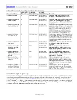
Bits Bit
Name Settings
Description
Reset
Access
2
SW2
SW2 Switch Control Active High.
0x0
R/W
0
Open
switch.
1
Close
switch.
1
SW1
SW1 Switch Control Active High.
0x0
R/W
0
Open
switch.
1
Close
switch.
0
SW0
SW0 Switch Control Active High.
0x0
R/W
0
Open
switch.
1
Close
switch.
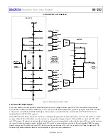
LPDAC0 DATA OUT REGISTER
Address: 0x400C2120, Reset: 0x00000000, Name: LPDACDAT0
Table 113. Bit Descriptions for LPDACDAT0
Bits Bit
Name
Settings
Description
Reset
Access
[31:18] Reserved
Reserved.
0x0 R
[17:12] DACIN6
6-Bit Value, 1 LSB = 34.375 mV. A low power DAC0 6-bit output data register value
between 0 and 0x3F is expected to set 6-bit output voltage.
0x0 R/W
0
0.2
V.
111111
2.366
V.
[11:0] DACIN12
12-Bit Value, 1 LSB = 537 μV. A low power DAC0 12-bit output data register value
between 0 and 0xFFF is expected to set 12-bit output voltage.
0x0 R/W
0
0.2
V.
0xFFF
2.4
V.
LPDAC0 SWITCH CONTROL REGISTER
Address: 0x400C2124, Reset: 0x00000000, Name: LPDACSW0
Table 114. Bit Descriptions for LPDACSW0
Bits Bit
Name Settings
Description
Reset
Access
[31:6] Reserved
Reserved.
0x0
R
5
LPMODEDIS
Switch Control. Controls switches connected to the output of low power DAC0.
0x0
R/W
0
Switches connected to output of low power DAC configured via LPDACCON0,
Bit 5. Default.
1
Overrides LPDACCON0, Bit 5. Switches connected to the low power DAC0
output are controlled via LPDACSW0, Bits[4:0].
4
SW4
LPDAC0 SW4 Control.
0x0
R/W
0
Disconnect direct connection of VBIAS0 DAC output to positive input of low
power Amplifier 0. Default.
1
Connect VBIAS0 DAC output directly to positive input of low power Amplifier 0.
3
SW3
LPDAC0 SW3 Control.
0x0
R/W
0
Disconnect VBIAS0 DAC output from low-pass filter and VBIAS0 pin.
1
Connect VBIAS0 DAC output to the low-pass filter and VBIAS0 pin. Default.
2
SW2
LPDAC0 SW2 Control.
R/W
0
Disconnect direct connection of VZERO0 DAC output to low power TIA0 positive
input. Default.
0x0
1
Connect VZERO0 DAC output directly to low power TIA0 positive input.
1
SW1
LPDAC0 SW1 Control.
0x0
R/W
0
Disconnect VZERO0 DAC output from the low-pass filter and VZERO0 pin.
1
Connect VZERO0 DAC output to the low-pass filter and VZERO0 pin. Default.
0
SW0
LPDAC0 SW0 Control.
0x0
R/W
0
Disconnect VZERO0 DAC output from high speed TIA positive input. Default.
1
Connect VZERO0 DAC output to the high speed TIA positive input.


