


UG-1262
Rev. B | Page 60 of 312
The low power TIA outputs have a low-pass filter. The resistor connecting the TIA output to the input mux is typically 1 MΩ with a
recommended external low-pass filter capacity of 4.7 μF resulting in a very low cutoff frequency. This resistor is labeled RFILTER in
Figure 10. For more details on how to set up the sensor bias voltage, see the Low Power DACs section.
ADC INPUT CIRCUIT
Figure 8 shows a basic view of the ADC input stages from the ADC mux to the ADC.
The ADC input mux is programmable to select from up to 34 positive input channels. Features of the input mux include the following:
The positive input can be selected via ADCCON, Bits[5:0].
The negative input is nominally expected to be the 1.11 V reference source, selected via ADCCON, Bits[12:8] = 0b01000.
An optional PGA can be selected to amplify the positive voltage input. The PGA or instrumentation amplifier are enabled via
AFECON, Bit 10. The gain setting is configured via ADCCON, Bits[18:16].
The output of the gain stage goes through an antialias filter. The cutoff frequency of the antialias filter is set by PMBW, Bits[3:2]. Set
the cutoff frequency to suit the input signal bandwidth. See the ADC, High Speed DAC, and Associated Amplifiers Operating Mode
Configuration section for more details.
The ADC output code is calibrated with an offset and gain correction factor. This digital adjustment factor occurs automatically. The
offset and gain correction register used depends on the ADC input channel selected. See the ADC Calibration section for more details.
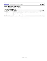
ADC POSTPROCESSING FILTER OPTIONS
Figure 11 shows an overview of the postprocessing options for ADC results.
DATA FIFO
SINC3 FILTER
OSR5/4/2
AD
C
G
A
IN
AN
D
O
FFS
ET
SI
N
C
2
FI
L
T
E
R
C
O
NFI
G
U
RAB
LE
OS
R
60Hz
NOTCH
GA
IN
CO
RR
ECTI
O
N
DFT
8k~16k
POINT
DFT_CORDIC
HANNING
ADC
MU
X
800kHz/
1.6MHz
APB
DIE TO DIE
MU
X
50Hz
NOTCH
MU
X
STATISTICS
ADCFILTER
CON[13:12]
ADCFILTER
CON[11:8]
ADCFILTER
CON[6]
ADCFILTER
CON[4]
MU
X
1.6MHz
0.8MHz
ADCFILTER
CON[0]
MU
X
AVG2/4
/8/16
ADCFILTER
CON[7]
DFTCON[0]
DFTCON[21:20]
DFTCON[7:4]
ADCFILTER
CON[15:14]
STATS
CON[6:4]
AFECON[15]
16
675
-0
11
Figure 11. ADC Postprocessing Filter Options
Sinc3 Filter
The input is the raw ADC codes at a rate of 800 kHz if the 16 MHz oscillator is selected on the analog die, or 1.6 MHz if the 32 MHz
oscillator is selected on the analog die.
To enable the sinc3 filter, ensure that ADCFILTERCON, Bit 6 = 0. The filter decimation rate is programmable. The recommended
decimation or oversampling rate (OSR) is 4. The OSR is controlled by ADCFILTERCON, Bits[13:12]. The input rate is 200 kSPS in
normal mode if the 16 MHz oscillator is selected, and 400 kSPS in high speed mode if the 32 MHz oscillator is selected.
If selected, the sinc3 filter output can be read via the ADCDAT register. When changing the ADC input channels or when changing the
ADC update rates via ADCFILTERCON, the user must reset the sinc3 filter. If sinc3 filter is not reset, ADC samples with the new
settings are inaccurate.
The following are example instructions:
pADI_AFE->AFECON &= (~(BITM_AFE_AFECON_ADCCONVEN)); // Clear AFECON[8]
pADI_AFE->AFECON |= BITM_AFE_AFECON_ADCCONVEN; // Set AFECON[8]
Sinc2 Filter
The input is the gain or offset adjusted codes from the sinc3 filter or from the ADC. The input rate is 800 kSPS if coming directly from the
ADC when the 16 MHz oscillator is selected, 1.6 MSPS if coming directly from the ADC when the 32 MHz oscillator is selected, and 400 kSPS
or 160 kSPS if coming directly from the sinc3 filter output.
To enable the sinc2 filter, set AFECON, Bit 16 = 1. The output rate from the sinc2 filter is programmable via ADCFILTERCON,
Bits[11:8]. The decimation rate is a minimum of divide by 22 to a maximum of divide by 1333. If selected, the sinc2 filter output can be
read via the SINC2DAT register.


