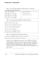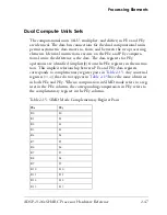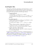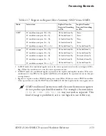
Alternate (Secondary) Data Registers
2-40
ADSP-2126x SHARC Processor Hardware Reference
•
S0
through
S15
always refer to PEy registers for data move instruc-
tions, whether the DSP is in SISD or SIMD mode.
For more information on SISD and SIMD computational operations, see
“Secondary Processing Element (PEy)” on page 2-45
tion on ADSP-2126x assembly language, see
SHARC Processor
Programming Reference
.
Alternate (Secondary) Data Registers
Each register file has an alternate register set. To facilitate fast context
switching, the DSP includes alternate register sets for data, results, and
data address generator registers. Bits in the
MODE1
register control when
alternate registers become accessible. While inaccessible, the contents of
alternate registers are not effected by DSP operations. Note that there is a
maximum one cycle latency from the time when writes are made to
MODE1
and the point when an alternate register set can be accessed. The alternate
register sets for data and results are described in this section. For more
information on alternate data address generator registers, see DAG
nate (Secondary) DAG Registers” on page 4-6
Bits in the
MODE1
register can activate independent alternate data register
sets: the lower half (
R0
-
R7
and
S0
-
S7
) and the upper half (
R8
-
R15
and
S8
-
S15
). To share data between contexts, a program places the data to be
shared in one half of either the current processing element’s register file or
the opposite processing element’s register file and activates the alternate
register set of the other half. For information on how to activate alternate
data registers, see the description of the
MODE1
register below.
Each multiplier has a primary or foreground (
MRF
) register and alternate or
background (
MRB
) results register. A bit in the
MODE1
register selects which
result register receives the result from the multiplier operation, swapping
which register is the current
MRF
or
MRB
. This swapping facilitates context
switching. Unlike other registers that have alternates, both
MRF
and
MRB
are
accessible at the same time. All fixed-point multiplies can accumulate
Содержание ADSP-21261 SHARC
Страница 30: ...Contents xxx ADSP 2126x SHARC Processor Hardware Reference ...
Страница 40: ...Register Diagram Conventions xl ADSP 2126x SHARC Processor Hardware Reference ...
Страница 58: ...Differences From Previous SHARCs 1 18 ADSP 2126x SHARC Processor Hardware Reference ...
Страница 112: ...Secondary Processing Element PEy 2 54 ADSP 2126x SHARC Processor Hardware Reference ...
Страница 178: ...Summary 3 66 ADSP 2126x SHARC Processor Hardware Reference ...
Страница 204: ...DAG Instruction Summary 4 26 ADSP 2126x SHARC Processor Hardware Reference ...
Страница 322: ...Setting Up DMA 7 32 ADSP 2126x SHARC Processor Hardware Reference ...
Страница 436: ...SPORT Programming Examples 9 86 ADSP 2126x SHARC Processor Hardware Reference ...
Страница 521: ...ADSP 2126x SHARC Processor Hardware Reference 11 31 Input Data Port rts IDP_ISR end ...
Страница 522: ...Input Data Port Programming Example 11 32 ADSP 2126x SHARC Processor Hardware Reference ...
Страница 590: ...Timer Programming Examples 14 20 ADSP 2126x SHARC Processor Hardware Reference ...
Страница 796: ...I O Processor Registers A 174 ADSP 2126x SHARC Processor Hardware Reference ...
Страница 800: ...B 4 ADSP 2126x SHARC Processor Core Manual ...
Страница 846: ...Index I 36 ADSP 2126x SHARC Processor Hardware Reference ...


