ADSP-2126x SHARC Processor Hardware Reference
3-9
Program Sequencer
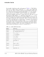
cache hit. The same instruction does generate a hit and can be taken from
the cache after the cache is enabled.
If the cache freeze bit of the
MODE2
register is set by a program memory
data access instruction
n
, then the
n+2
instruction is cached. This results
from the effect latency of the
MODE2
register.
When a program changes the cache mode, an instruction contain-
ing a program memory data access must not be placed directly after
a cache enable or cache disable instruction. This is because the DSP
must wait at least one cycle before executing the PM data access. A
program should have a
NOP
or other non-conflicting instruction
inserted after the cache enable instruction.
Optimizing Cache Usage
Cache operation is usually efficient and requires no intervention. How-
ever, certain ordering of instructions can work against the cache’s
architecture, reducing its efficiency. When the order of PM data accesses
and instruction fetches continuously displaces cache entries and loads new
entries, the cache does not operate efficiently. Rearranging the order of
these instructions remedies this inefficiency. Optionally, a dummy PM
read can be inserted to trigger the cache.
When a cache miss occurs, the needed instruction is loaded into the cache
so that if the same instruction is needed again, it will be there (that is, a
cache hit will occur). However, if another instruction whose address is
mapped to the same set displaces this instruction, a cache miss occurs. The
LRU
bits help to reduce this possibility since at least two other instructions,
mapped to the same set, are needed before an instruction is displaced. If
three instructions mapped to the same set are all needed repeatedly, cache
efficiency (that is, “hit rate”) can go to zero. To solve this problem, move
one or more instructions to a new address that is mapped to a different
cache set.
Содержание ADSP-21261 SHARC
Страница 30: ...Contents xxx ADSP 2126x SHARC Processor Hardware Reference ...
Страница 40: ...Register Diagram Conventions xl ADSP 2126x SHARC Processor Hardware Reference ...
Страница 58: ...Differences From Previous SHARCs 1 18 ADSP 2126x SHARC Processor Hardware Reference ...
Страница 112: ...Secondary Processing Element PEy 2 54 ADSP 2126x SHARC Processor Hardware Reference ...
Страница 178: ...Summary 3 66 ADSP 2126x SHARC Processor Hardware Reference ...
Страница 204: ...DAG Instruction Summary 4 26 ADSP 2126x SHARC Processor Hardware Reference ...
Страница 322: ...Setting Up DMA 7 32 ADSP 2126x SHARC Processor Hardware Reference ...
Страница 436: ...SPORT Programming Examples 9 86 ADSP 2126x SHARC Processor Hardware Reference ...
Страница 521: ...ADSP 2126x SHARC Processor Hardware Reference 11 31 Input Data Port rts IDP_ISR end ...
Страница 522: ...Input Data Port Programming Example 11 32 ADSP 2126x SHARC Processor Hardware Reference ...
Страница 590: ...Timer Programming Examples 14 20 ADSP 2126x SHARC Processor Hardware Reference ...
Страница 796: ...I O Processor Registers A 174 ADSP 2126x SHARC Processor Hardware Reference ...
Страница 800: ...B 4 ADSP 2126x SHARC Processor Core Manual ...
Страница 846: ...Index I 36 ADSP 2126x SHARC Processor Hardware Reference ...

