


6–54
Chapter 6: IP Core Interfaces
Physical Layer Interface Signals
Stratix V Hard IP for PCI Express
June 2012
Altera Corporation
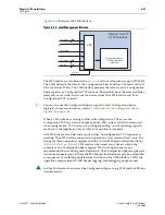
The following sections describe signals for the serial or parallel PIPE interlaces. The
PIPE interface is only available for simulation.
Serial Interface Signals
describes the serial interface signals.
f
Refer to
Pin-out Files for Altera Devices
for pin-out tables for all Altera devices in
,
.txt
, and
.xls
formats.
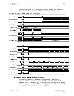
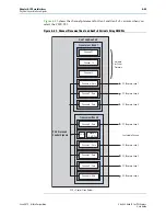
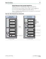
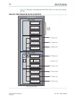
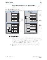
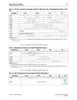
Channel Placement for Gen1 and Gen2 Using CMU PLL
shows the channel placement for Gen1 and Gen2 ×1 and ×4 variants
when you select the CMU PLL.
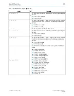
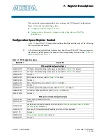
Table 6–30. 1-Bit Interface Signals
Signal I/O
Description
tx_out
[7:0]
O
Transmit input. These signals are the serial outputs of lanes 7–0.
rx_in
I
Receive input. These signals are the serial inputs of lanes 7–0.
Note to
:
(1) The ×1 IP core only has lane 0. The ×4 IP core only has lanes 3–0.
Figure 6–41. Channel Placement Gen1 and Gen2 x1 and x4 Variants
Gen1 and Gen 2 x1
T
r
ansceive
r
Bank
LCD
LCD = Local Clock Divider
Channel 0 -
Data
Channel 1 - CMU PLL
Channel 2 - Data
Channel 4
Channel 5
PCIe Lane 0
Channel 3
Gen1 and Gen2 x4
Channel 0 - Data
Other
Protocols
Other
Protocols
Channel 2 - Data
Channel 1 - CMU PLL
Channel 5
Channel 3 - Data
Channel 4 - Data
T
r
ansceive
r
Bank
PCIe Lane 0
PCIe Lane 1
Unavailable chann
PCIe Lane 2
PCIe Lane 3
PCS Clock and
Con
tr
ol Signals
PCS Clock and
Con
tr
ol Signals