Chapter 1: Nios II Hardware Development
1–27
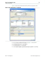
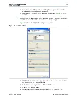
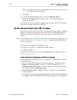
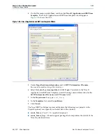
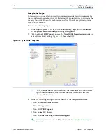
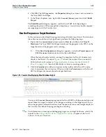
Creating the Design Example
May 2011
Altera Corporation
Nios II Hardware Development Tutorial
2. In the
Family
list, select the FPGA family that matches your board.
1
If prompted to remove location assignments, do so.
3. Under
Target device
, select
Specific device selected in 'Available devices' list
.
4. Under
Available devices
, select the exact device that matches your board.
1
If prompted to remove location assignments, do so.
5. Click
OK
to accept the device assignment.
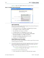
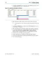
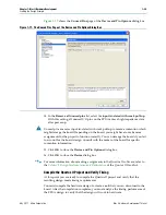
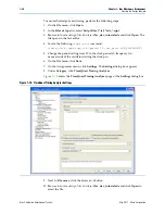
shows an example of the
Device
dialog box.
To assign the FPGA pin locations, perform the following steps:
1. On the Processing menu, point to
Start
, and click
Start Analysis & Elaboration
to
prepare for assigning pin locations. The analysis starts by displaying a “data not
available” message and can take several minutes. A confirmation message box
appears when analysis and elaboration completes.
2. Click
OK
.
3. On the Assignments menu, click
Pin Planner
. The Quartus II Pin Planner appears.
4. In the
Node Name
column, locate
PLD_CLOCKINPUT
.
Figure 1–15. Assigning a Device in the Quartus II Settings Dialog Box


