Altera Cyclone III FPGA Скачать руководство пользователя страница 11

Altera Corporation 

Reference Manual

2–3

October 2007

Cyclone III FPGA Starter Board

Board Components & Interfaces
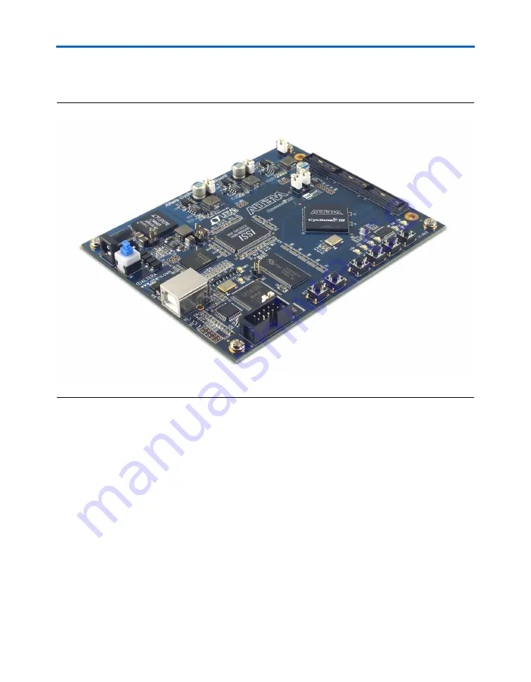
Figure 2–2

 shows the diagonal view of the Cyclone III FPGA starter 

board.

Figure 2–2. Diagonal View of the Cyclone III FPGA Starter Board

Содержание Cyclone III FPGA

Страница 1: ...101 Innovation Drive San Jose CA 95134 www altera com Cyclone III FPGA Starter Board Reference Manual Document Date October 2007...

Страница 2: ...hts and copyrights Altera warrants performance of its semiconductor products to current specifications in accordance with Altera s standard warranty but reserves the right to make changes to any produ...

Страница 3: ...rd Overview 2 1 Featured Device 2 5 Clocking Circuitry 2 6 Jumpers 2 7 Interfaces 2 8 USB Interface 2 8 HSMC Expansion Connector 2 9 General User Interfaces 2 10 Push Buttons 2 13 LEDs 2 14 Memory 2 1...

Страница 4: ...iv Altera Corporation Preliminary October 2007 Contents Stratix Device Handbook Volume 1...

Страница 5: ...ughter cards that allow you to expand the functionality of the board f For the latest information about available HMSC daughter cards go to www altera com products devkits kit index html The main feat...

Страница 6: ...I O pins for communicating with HSMC daughter cards General user interface Four user LEDs Two board specific LEDs Push buttons System reset User reset Four general user push buttons Memory subsystem S...

Страница 7: ...1 Cyclone III FPGA Starter Board Handling the Board When handling the board it is important to observe the following precaution c Static Discharge Precaution Without proper anti static handling the bo...

Страница 8: ...1 4 Reference Manual Altera Corporation Cyclone III FPGA Starter Board October 2007 Handling the Board...

Страница 9: ...Altera HSMC expansion connector General user interfaces Memory Power supply Statement of China RoHS compliance 1 Board schematics the physical layout database and manufacturing files for the Cyclone...

Страница 10: ...ne III FPGA Starter Board Cyclone III Device U1 User Push Button Switches User LEDs USB UART U8 HSMC Connector J1 DC Power Input J2 Power Switch SW1 USB Connector J3 Configuration Done LED 32 Mbyte DD...

Страница 11: ...ence Manual 2 3 October 2007 Cyclone III FPGA Starter Board Board Components Interfaces Figure 2 2 shows the diagonal view of the Cyclone III FPGA starter board Figure 2 2 Diagonal View of the Cyclone...

Страница 12: ...the Cyclone III device for external FPGA configuration and communication with applications running on the FPGA 2 8 Input HSMC Connector J1 Header for connecting the HSMC interface 2 9 Configuration Re...

Страница 13: ...A Starter Board Part 2 of 2 Type Component Interface Board Reference Description Page Table 2 2 Cyclone III Device Features Architectural Feature Results Altera s third generation of low cost FPGAs Lo...

Страница 14: ...ks are generated using the Cyclone III device s phase locked loops PLLs The dedicated PLLs are used to distribute the flash SSRAM and HSMC clocks Table 2 4 shows the clock pinout Table 2 3 Cyclone III...

Страница 15: ...V9 32 MB DDR Note Reference numbers are FPGA pin numbers Out A1 C14 D14 V18 U18 In A9 F18 F17 N18 N17 U2 V2 A2 H4 Table 2 5 Board Jumpers Part 1 of 2 JumperBoard Reference Jumper Operational Descript...

Страница 16: ...ne III device s dedicated JTAG port The 5 V supply for the FTDI device is drawn from the USB connection The rest of the circuit operates on 3 3 V supply with 100 mA maximum and 1 8 V supply with 900 m...

Страница 17: ...ble 2 6 lists the ordering codes and shows the relationship between the standard Samtec Q series connectors and the modified parts ordering codes The board provides both 12 V unregulated and 3 3 V reg...

Страница 18: ...u to fully leverage the I O capabilities of the Cyclone III device the following are available on the board remaining I Os are connected to additional board resources Push buttons System and user rese...

Страница 19: ...put 2 5 V 155 HSMC_CLKIN_p2 N17 Input 2 5 V 156 HSMC_CLKOUT_n2 V18 Output 2 5 V 157 HSMC_CLKIN_n2 N18 Input 2 5 V 158 HSMC_D0 H6 Bidirectional 2 5 V 41 HSMC_D1 D3 Bidirectional 2 5 V 42 HSMC_D2 M5 Bid...

Страница 20: ...ional 2 5 V 89 HSMC_RX_p7 L4 Bidirectional 2 5 V 90 HSMC_TX_n7 L1 Bidirectional 2 5 V 91 HSMC_RX_n7 L3 Bidirectional 2 5 V 92 HSMC_TX_p8 M2 Bidirectional 2 5 V 101 HSMC_RX_p8 P2 Bidirectional 2 5 V 10...

Страница 21: ...nal 2 5 V 134 HSMC_TX_p14 P17 Bidirectional 2 5 V 137 HSMC_RX_p14 R17 Bidirectional 2 5 V 138 HSMC_TX_n14 P18 Bidirectional 2 5 V 139 HSMC_RX_n14 R18 Bidirectional 2 5 V 140 HSMC_TX_p15 R5 Bidirection...

Страница 22: ...ed to the DEV_CLRn pin on the FPGA The DEV_CLRn setting is a pin option in the Quartus II software that you must enable to function as DEV_CLRn instead of a standard I O User Push Buttons The four use...

Страница 23: ...rd s power is on and working The configuration done LED illuminates when the FPGA is programmed Configuration LED The Conf_Done LED illuminates when the FPGA is successfully configured with any design...

Страница 24: ...B85 Note to Table 2 12 1 The Cyclone III Starter board comes assembled with a 128 Mb flash device but has been pinned out for a flash chip as large as 512 Mb in size Therefore leave address lines 24 a...

Страница 25: ...flash_sram_dq4 B7 Bidirectional 2 5 V E5 flash_sram_dq5 C5 Bidirectional 2 5 V G5 flash_sram_dq6 E8 Bidirectional 2 5 V G6 flash_sram_dq7 A4 Bidirectional 2 5 V H7 flash_sram_dq8 B4 Bidirectional 2 5...

Страница 26: ...D40CTP G5PP Table 2 15 DDR SDRAM Pinout Part 1 of 2 Signal Name FPGA Pin Direction Type U4 DDR Pin ddr_dqs0 U3 Bidirectional SSTL 2 16 ddr_dqs1 T8 Bidirectional SSTL 2 51 ddr_dm0 V3 Output SSTL 2 47 d...

Страница 27: ...l SSTL 2 7 ddr_dq4 P9 Bidirectional SSTL 2 8 ddr_dq5 U6 Bidirectional SSTL 2 10 ddr_dq6 V6 Bidirectional SSTL 2 11 ddr_dq7 V7 Bidirectional SSTL 2 13 ddr_dq8 U13 Bidirectional SSTL 2 54 ddr_dq9 U12 Bi...

Страница 28: ...flash_sram_a12 A11 Output 2 5 V 48 flash_sram_a13 B11 Output 2 5 V 49 flash_sram_a14 C10 Output 2 5 V 50 flash_sram_a15 D10 Output 2 5 V 81 flash_sram_a16 E10 Output 2 5 V 82 flash_sram_a17 C9 Output...

Страница 29: ...sh_sram_dq22 A17 Bidirectional 2 5 V 12 flash_sram_dq23 D16 Bidirectional 2 5 V 13 flash_sram_dq24 C12 Bidirectional 2 5 V 18 flash_sram_dq25 A18 Bidirectional 2 5 V 19 flash_sram_dq26 F8 Bidirectiona...

Страница 30: ...s circuit refer to the Cyclone III FPGA Starter Kit Getting Started User Guide Table 2 18 Board Regulators Output Voltage V Variance mV MAX Current A Board Access Point Regulator Board Reference Linea...

Страница 31: ...PBB Polybrominated diphenyl Ethers PBDE Cyclone III FPGA starter board X 0 0 0 0 0 12 V power supply 0 0 0 0 0 0 Type A B USB cable 0 0 0 0 0 0 User guide 0 0 0 0 0 0 Notes to Table 2 19 1 0 indicates...

Страница 32: ...2 24 Reference Manual Altera Corporation Cyclone III FPGA Starter Board October 2007 Statement of China RoHS Compliance...

Страница 33: ...inor corrections in Chapter 2 Moved front matter to back All April 2007 1 0 0 First publication Contact 1 Contact Method Address Technical support Website www altera com support Technical training Web...

Страница 34: ...ng Title References to sections within a document and titles of on line help topics are shown in quotation marks Example Typographic Conventions Courier type Signal and port names are shown in lowerca...

Отзывы: