background image

ADM-PCIE-7V3
 Getting Started Guide

3 Xilinx OpenCL

This guide only covers a few basic points on the use of the board with Xilinx OpenCL.  To use the board with

Xilinx OpenCL, switch SW1-1 must be set to on to enable Xilinx mode.  This will cause the board to boot up with

the Xilinx OpenCL bitstream.  This will appear as a different PCIe device from the HDL designed bitstreams used

in AD mode.  To access the card, follow the instructions provided in the Xilinx OpenCL documentation for

installing the OpenCL driver and for configuring the card to run OpenCL kernels. If the default OpenCL bitstream

has not been pre-programmed into the OpenCL area of the flash, you may need perform this step using a JTAG

cable.

Page 5

Xilinx OpenCL
ad-ug-0033_v1_4.pdf

Содержание ADM-PCIE-7V3

Страница 1: ...ADM PCIE 7V3 Getting Started Guide Revision V1 4 07 01 15...

Страница 2: ...form without prior written consent from Alpha Data Parallel Systems Ltd Head Office Address 4 West Silvermills Lane Edinburgh EH3 5BD UK Telephone 44 131 558 2600 Fax 44 131 558 2700 email sales alpha...

Страница 3: ...emory Interface Generator 12 5 2 AXI 4 Reference designs demonstrating PCIe and Memory 17 5 2 1 Basic AXI 4 PCIE Reference Design 17 5 2 2 AXI 4 Reference Design with Memory Interfaces 19 5 3 SDK FPGA...

Страница 4: ...tency It also supports 2 SATA ports for users who require very large but locally accessible storage The boards primary development language and environment is the Xilinx OpenCL development kit This is...

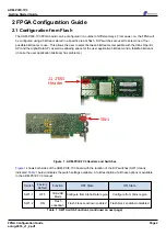
Страница 5: ...d a failsafe bitstream in case the user application bitstream has problems J1 JTAG Header SW1 Figure 1 ADM PCIE 7V3 Headers and Switches Figure 1 shows both sides of the ADM PCIE 7V3 board with the lo...

Страница 6: ...lished in a number of different ways The recommended way is to boot the board in AD mode and use the flash program to write the bitstream to the specified flash address Writing the flash can also be a...

Страница 7: ...ing IPROG reconfiguration as detailed in Xilinx UG470 7 Series FPGAs Configuration User Guide In this case a start address of a bitstream in flash can be written to the ICAPE2 component within the FPG...

Страница 8: ...ilinx OpenCL bitstream This will appear as a different PCIe device from the HDL designed bitstreams used in AD mode To access the card follow the instructions provided in the Xilinx OpenCL documentati...

Страница 9: ...15 The Linux driver can be downloaded from ftp ftp alpha data com pub admxrcg3 linux adb3 driver linux 1 4 15 tar gz and the Windows driver can be downlaoded from ftp ftp alpha data com pub admxrcg3 w...

Страница 10: ...sting host examples with reference bitstreams In this section the use of host example code to control the card will be demonstrated stepping through the commands required to start the driver and run m...

Страница 11: ...Virtual size 0x400000 Window 2 ADM PCIE 7V3 spec Bus base 0xF7C00000 size 0x1000 Local base 0x0 size 0x0 Virtual size 0x1000 Window 3 ADB3 bridge regis Bus base 0xF7C01000 size 0x1000 Local base 0x0 s...

Страница 12: ...C 0x00000000_00000070 4321dcba 4321dcba 4321dcba 4321dcba C C C C root jura2 linux dump dump rd 2 0 0x80 Window 2 offset 0x0 mapped 0x7f334a95e000 Dump of memory at 0x7f334a95e000 128 0x80 bytes 00 04...

Страница 13: ...10000 kiB Useable region is 0x0 0x3FFFFFF root jura2 linux flash flash program 0 simple admpcie7v3 7vx690t bit Target FPGA is device 7vx690tffg1157 Flash type is Numonyx Axcell P30 Symm bl 65536 0x100...

Страница 14: ...0000070 0000001c 0000001d 0000001e 0000001f 0x00000000_00000080 00000020 00000021 00000022 00000023 0x00000000_00000090 00000024 00000025 00000026 00000027 0x00000000_000000a0 00000028 00000029 000000...

Страница 15: ...ivado and Select create new project Select RTL Project Click next on the pages for Add Sources Add Existing IP and Add Constraints For Default Part select xc7vx690tffg1157 2 and click next Then click...

Страница 16: ...o 2 On the controller options pages Select 1500ps for the Clock Period This will configure the controller to run the external memory at 1333MHz For the memory type select SODIMMs and select the MT18KS...

Страница 17: ...e On the memory options page set the input clock period to 2500ps 400MHz and change RTT to RZQ 6 Leave FPGA options unchanged In Pin Bank Selection Mode select Fixed Pin Out Page 14 FPGA Firmware Refe...

Страница 18: ...ve low sys_rst connect to W27 the boards PCIe reset pin Also connect init_calib_complete to AC33 and tg_compare_error to U30 This will light a green LED if the calibration completes or a red LED if th...

Страница 19: ...CKAGE_PIN AA24 get_ports dram_0_on set_property IOSTANDARD LVCMOS18 get_ports dram_0_on set_property PACKAGE_PIN AB25 get_ports dram_1_on set_property IOSTANDARD LVCMOS18 get_ports dram_1_on Page 16 F...

Страница 20: ...dress bits running at 250MHz To connect with IP that is not compatible with this profile the data width clock domain and protocol converters supplied in the Xilinx Vivado IP catalog should be used The...

Страница 21: ...7ff3_0xe8f03030 00000000 00000000 00000000 00000000 0x00007ff3_0xe8f03040 00000000 00000000 00000000 00000000 0x00007ff3_0xe8f03050 00000000 00000000 00000000 00000000 0x00007ff3_0xe8f03060 00000000 0...

Страница 22: ...though the n 0 flag should be used to prevent reports of spurious arros root jura2 simpledma simpledma n 0 Reading using DMA channel 0 at OCP address 0x0 Dump of data read from OCP address 0x0 0x0 B 0...

Страница 23: ...per Some external LEDs are connected to indicate the status of the MIG training D2 and D3 should light up green if the Memory PLLs achieve lock for each bank If memory training and calibration fail Re...

Страница 24: ...dump rd 0 0x0 0x40 Window 0 offset 0x0 mapped 0x0x7f95902df000 Dump of memory at 0x0x7f95902df000 64 0x40 bytes 00 04 08 0c 0x00007f95_0x902df000 00000000 00000000 00000000 00000000 0x00007f95_0x902d...

Страница 25: ...t jura2 dump wd 0 0x00000 0x40 Window 0 offset 0x0 mapped 0x0x7f11e60c8000 0x0 5 0x4 6 0x8 7 0xC 8 0x10 1 0x14 2 0x18 3 0x1C 4 0x20 a 0x24 b 0x28 c 0x2C d 0x30 e 0x34 f 0x38 0 0x3C 1 root jura2 dump r...

Страница 26: ...00 00000000 0x00000000_00000060 00000000 00000000 00000000 00000000 0x00000000_00000070 00000000 00000000 00000000 00000000 0x00000000_00000080 00000000 00000000 00000000 00000000 0x00000000_00000090...

Страница 27: ...Dump of data read from OCP address 0x0 0x0 B 00 04 08 0c Measuring throughput Throughput from host to FPGA is 5422 9 MiB s Throughput from FPGA to host is 4997 6 MiB s PASSED root jura2 simpledma sim...

Страница 28: ...e conforming to the OCP standard This is similar in function to memory mapped AXI4 and can be interfaced relatively easily with some AXI 4 profiles These examples will prove most useful for existing A...

Страница 29: ...le disabled size 4M Capabilities 80 Power Management version 3 Flags PMEClk DSI D1 D2 AuxCurrent 0mA PME D0 D1 D2 D3hot D3cold Status D0 NoSoftRst PME Enable DSel 0 DScale 0 PME Capabilities 90 MSI En...

Страница 30: ...ed bitstream If the FPGA should have been configured from a bitstream stored in flash please check the settings of switch SW1 Note that if the boards has been configured with the OpenCL bitstream it w...

Страница 31: ...001f 00000011 0x00007f00_0x11c05010 00000002 a5100100 220d4000 003fffff 0x00007f00_0x11c05020 00000000 00000000 003fffff 00000000 0x00007f00_0x11c05030 00000000 00000000 00000000 00000000 0x00007f00_0...

Страница 32: ...se SDK 1 7 0 07 01 15 1 4 modified designs to support 2014 4 Address 4 West Silvermills Lane Edinburgh EH3 5BD UK Telephone 44 131 558 2600 Fax 44 131 558 2700 email sales alpha data com website http...

Отзывы: