
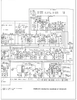

3.3
FIRST MIXER AND BANDPASS IF
The output of the RF Amplifier is applied to the gate of the first mixer Q4. At the same time the
output of the HFO coupled thru T4 is applied to the source of the first mixer. The two signals are
mixed and their products are selected in the drain circuit of Q4. The circuit in the drain of Q3 is
tuned as a bandpass circuit passing all frequencies between 2.920 MHz and 2.420 MHz. This is
the frequency range of the 500 KHz bandpass IF. The transformers L8, 9 and Ll0 and their asso-
ciated components comprise the bandpass IF. The output of this IF is applied to the base of Q8,
the second mixer.
3.4
SECOND MIXER AND VARIABLE FREQUENCY OSCILLATOR
The second mixer combines the output of the bandpass IF with the output of the variable fre-
quency oscillator (VFO) to produce the 455 KHz IF.
The VFO produces the required frequencies for tuning LSB, USB, CW and AM signals. Inductor
T7 parallels capacitor VC6, in the frequency-determining network. The output frequency is low-
ered causing the VFO to tune from 3.375-2.875 MHz.
The mixing products of the bandpass IF and VFO are selected in the collector circuit of Q8 (sec-
ond mixer). The output of the VFO is provided at the rear panel at J4. Here the VFO is isolated
by emitter follower (Q10).
3.5
455 KHz IF DETECTOR CIRCUITS AND NOISE LIMITER
Immediately following the 2nd mixer (Q8) are the mechanical Filters (MF1, MF2). Output from
the MF1 is amplified by Q13 and connects to MF2 and is tuned by the three transformers T9,
T10 and T11. The signal is taken from the secondary of T11 to be detected and used as the AGC
voltage.
The AM detector, diode D5, also gets its signal from the secondary of T11 and is coupled to the
noise limiter (D4). This noise limiter only functions in the AM mode when its output is delivered
through the function switch, on to the AF GAIN and to the 1st audio amplifier.
The detection of CW & SSB signals is accomplished by D8, D9. Dl0 and D11. These four diodes
comprise a balanced demodulator circuit. The audio is developed from the product detection of
the incoming 455 KHz signal and the output of the BFO, which may come from the crystal con-
trolled SSB oscillator, and its output is delivered to AM preamplifier (Q17). The output of the
AM preamplifier is coupled thru C79 to Function switch (SW3-d) to the AF gain control, VR3,
and on to the 1st audio amplifier.
-18-
Содержание SX-190
Страница 1: ......
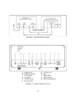
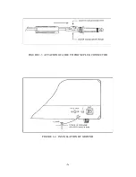
Страница 7: ...FIGURE 1 3 ATTACHING CABLE TO PHONE PLUG CONNECTOR FIGURE 1 4 INSTALLATION OF GROUND 6 ...
Страница 17: ... 16 ...
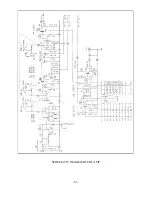
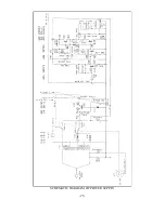
Страница 22: ...SCHEMATIC DIAGRAM OF RF AMP 21 ...
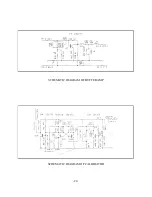
Страница 23: ...SCHEMATIC DIAGRAM OF BUFFER AMP SCHEMATIC DIAGRAM OF CALIBRATOR 22 ...
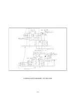
Страница 24: ...SCHEMATIC DIAGRAM OF VFO SECTION 23 ...
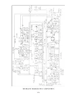
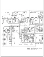
Страница 25: ...SCHEMATIC DIAGRAM OF I F AMP SECTION 24 ...
Страница 26: ...SCHEMATIC DIAGRAM OF POWER SUPPLY 25 ...
Страница 29: ......
Страница 30: ......
Страница 31: ......


