1
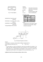
(2) Pin Configuration
.8 EEPROM AT24C08
(1) Features
Data EEPROM internally organized as 1024/2048
bytes and 64/128 pages×16 bytes
p
flexible page-b page
hardware write protection
- Additional protection EEPROM of 64/128 bits, 1 bit
per data page
- Protection setting for each data page by writing its
protection bit
- Protection management without switching WP in
Low power CMOS
Vcc=2.7 to 5.5V operation
Two wire serial interface bus, I
2
C-Bus compat
Filtered inputs for noise suppression with Schmitt
trigger
Clock frequency up to 400 kHz
High programming flexibility
- Internal programming voltage
- Self timed programming cycle including erase
- Byte-write and page-write programming, between 1 and 16 bytes
- Typical programming time 6 ms (<10 ms) for up to 16 bytes
- Endurance 10
6
cycles
1)
- Data retention 40 years
1)
- ESD protection 4000 V on all pins
8 pin DIP/DSO
packages
Available for extended temperature ranges
- Industrial: -40
- Automotive: -40
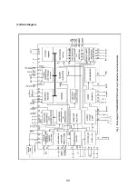
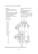
(3) Block Diagram
Fig. 22
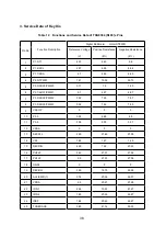
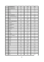
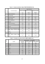
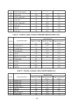
(4) Refer to Table 18 About Functions and Service Data of AT24C08’s Pins.
Page
rotection mode,
y-
p
ible
Fig. 21
High reliability
to +85
to +125
Page
Prot.Bit
EEPROM
34
Содержание 25CT23FSR
Страница 1: ...SERVICE MANUAL Models 25CT23FSR 29CT23FSR www akai ru COLOUR TV SET ...
Страница 16: ...2 Block Diagram for Supply Voltage System Fig 6 Block Diagram for Supply Voltage System 150 250V AC 50Hz 15 ...
Страница 21: ... 3 Block Diagram 7 20 ...
Страница 22: ...8 21 ...
Страница 23: ... 4 Pining 5 Refer to Table 12 about Functions and Data of the IC s Pins 9 22 ...
Страница 31: ... 2 Circuit Block Diagram Dwg MK 003 50mm Fig 18 Fig 17 3 Pin Configuration and Functions 30 ...
Страница 37: ...7 TDA938X PIN31 8 TDA938X PIN33 TDA938X PIN34 10 TDA938X PIN38 11 TDA938X PIN40 12 TDA938X PIN42 9 36 ...
Страница 46: ...CIRCUIT DIAGRAM JUC 820 975 JUC 820 591 JUC 820 725 JUC 820 644 APPENDIX ...

