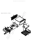
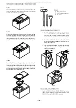
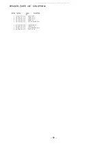
background image

– 44 –

ADJUSTMENT <DECK> (FX-NH2000)

< DECK  SECTION >

1. Tape Normal Speed Adjustment

Settings :

• Test tape :

TTA–100 (Tape center)

• Test point :

TP1 (Rch), TP2 (Lch)

• Adjustment location : SFR1

Method :

Play back the test tape and adjust SFR1 so that
the test point becomes 3000Hz 

±

 5Hz(FWD)

Then check REV speed is 3000Hz 

±

 45Hz.

2. High Speed Check

Settings :

• Test tape :

TTA–100 (Tape center)

• Test point :

TP1 (Rch), TP2 (Lch)

Method :

After normal speed adjustment, play back
(High speed) the test tape. Then check tape
speed is 6000Hz 

±

400Hz (FWD).

3. Head Azimuth Adjustment

Settings :

• Test tape :

TTA–300

• Test point :

TP1(Rch), TP2 (Lch)

• Adjustment location : Head azimuth

adjustment screw

Method :

Play back the 10kHz signal of the test tape and
adjust screw so that the output becomes
maximum.Next, perform on each FWD PLAY
and REV  PLAY mode.

4

PB  Sensitivity Adjustment (DECK1, DECK2)
Settings :

• Test tape :

TTA–200

• Test point :

TP1 (Rch), TP2 (Lch)

• Adjustment location : SFR301 (DECK1, Lch)

SFR302 (DECK1, Rch)
SFR303 (DECK2, Lch)
SFR304 (DECK2, Rch)

Method :

Play back the test tape and adjust SFRs so that
the output level of the test point becomes
245mV (DECK2), 260mV (DECK1).

5. PB  Frequency Response Check (DECK1, DECK2)

Settings :

• Test tape :

TTA–300

• Test point :

TP1 (Rch), TP2 (Lch)

Method :

Play back the 315Hz and 10kHz signals of the
test tape and check that the output ratio of the
10kHz signal with respect to that of the 315Hz
signal is 0dB .
Next, check that the Lch and Rch difference
level of 10kHz signal is less than 2dB.

6. REC/PB  Sensitivity Adjustment (DECK2)

Settings :

• Test tape :

TTA–602 (NORMAL)

• Test point :

TP1 (Rch), TP2 (Lch)

• Input signal :

1kHz (LINE  IN)

• Adjustment location : SFR305 (Lch)

SFR306 (Rch)

Method :

Apply a 1kHz signal and REC mode. Then adjust
OSC attenuator so that the output level at the
TP1, TP2 becomes 0dB (17mV). Record and
play back the 1kHz signals and adjust SFRs so
that the output is 0dB 

±

 0.5dB.

7. REC/PB  Frequency Response Adjustment (DECK2)

Settings :

• Test tape :

TTA–602 (NORMAL)

• Test point :

TP2 (Lch), TP1 (Rch)

• Input signal :

1kHz / 10kHz
(LINE  IN)

• Adjustment location : SFR351 (Lch)

SFR352 (Rch)

Method :

Apply a 1kHz signal and REC mode. Then adjust
OSC attenuator so that the output level at the
TP1, TP2 becomes 0dB (17mV). Record and
play back the 1kHz and 10kHz signals and adjust
SFRs so that the output level of the 10kHz
signals becomes 0dB 

±

 0.5dB with respect to

that of the 1kHz signal.

8. REC/PB  Frequency Response Check (DECK2)

Settings :

• Test tape :

TTA–615 (CrO2)

• Test point :

TP2 (Lch), TP1 (Rch)

• Input signal :

1kHz

Method :

Apply a 1kHz signal and REC mode. Then adjust
OSC attenuator so that the output level at the
TP1, TP2 becomes 0dB (17mV). Record and
play back the 1kHz signal and check that the output is
0dB 

±

 2.0dB.

9. REC/PB  Sensitivity Check (DECK2)

Settings :

• Test tape :

TTA–615 (CrO2)

• Test point :

TP2 (Lch), TP1 (Rch)

• Input signal :

1kHz (LINE OUT)

Method :

Apply a 1kHz signal and REC mode. Then adjust
OSC attenuator so that the output level at the
TP1, TP2 becomes 170mV. Record and
play back the 1kHz signal and check that the output is
0dB 

±

 2.0dB.

All manuals and user guides at all-guides.com

Содержание XR-H2000EZ

Страница 1: ...blishing and replaces Simple Manual XR H2000 EZ K S M Code No 09 005 427 6T2 If requiring information about the CD mechanism see Service Manual of AZG 1 ZD3RNDM S M Code No 09 001 335 3N8 XR H2000 CD PLAYER SYSTEM STEREO RECEIVER REMOTE CONTROL SX NDPH2100 MX NH2000 DX NH2000 CASSETTE DECK GRAPHIC EQUALISER SPEAKERS FX NH2000 GE NH2000 RC ZAS04 All manuals and user guides at all guides com a l l g...

Страница 2: ...N FRONT KEY 28 SCHEMATIC DIAGRAM MAIN FRONT KEY 29 FL GRID ASSIGNMENT AND ANODE CONNECTION 30 IC DESCRIPTION 31 32 MECHANICAL EXPLODED VIEW 1 1 33 MECHANICAL PARTS LIST 1 1 34 MODEL NO FX NH2000 ELECTRICAL MAIN PARTS LIST 35 36 TRANSISTOR ILLUSTRATION 37 WIRING 1 MAIN FRONT 1 FRONT 2 38 SCHEMATIC DIAGRAM MAIN FRONT 1 FRONT 2 DECK 39 WIRING 2 DECK 40 IC BLOCK DIAGRAM 41 IC DESCRIPTION 42 43 ADJUSTM...

Страница 3: ... sätt än vad som specificeras i denna bruksanvising kan användaren utsättas för osynling laserstrålning som överskrider gränsen för laserklass 1 PROTECTION OF EYES FROM LASER BEAM DURING SERVICING CAUTION Use of controls or adjustments or performance of proce dures other than those specified herin may result in hazardous radiation exposure ATTENTION L utillisation de commandes réglages ou procédur...

Страница 4: ...istortion 0 05 1 kHz 0 dB Wow and flutter Unmeasurable Dimensions of main unit 284 x 101 x 315 mm W x H x D Weight of main unit 2 3 kg CASSETTE DECK FX NH2000 Track format 4 tracks 2 channels stereo Frequency response Type II high CrO2 tape 50 Hz 16000 Hz Type I normal tape 50 Hz 15000 Hz Signal to noise ratio 60 dB Dolby B NR ON Type II tape peak level Recording system AC bias AC erase Heads Deck...

Страница 5: ...0 1 50 F C109 87 010 196 080 CHIP CAPACITOR 0 1 25 C110 87 010 196 080 CHIP CAPACITOR 0 1 25 C111 87 010 196 080 CHIP CAPACITOR 0 1 25 C112 87 010 196 080 CHIP CAPACITOR 0 1 25 C113 87 010 247 080 CAP ELECT 100 50V C114 87 010 385 080 CAP ELECT 220 25V C115 87 010 385 080 CAP ELECT 220 25V C116 87 010 247 080 CAP ELECT 100 50V C117 87 010 430 080 CAP ELECT 100 63 C118 87 010 263 080 CAP ELECT 100 ...

Страница 6: ... C910 87 012 368 080 C CAP S 0 1 50 F C911 87 012 141 080 CHIP CAPACITOR 0 22 16F C913 87 010 196 080 CHIP CAPACITOR 0 1 25 C920 87 012 157 080 C CAP S 330P 50 CH C921 87 012 157 080 C CAP S 330P 50 CH C922 87 012 157 080 C CAP S 330P 50 CH C923 87 012 157 080 C CAP S 330P 50 CH C924 87 012 157 080 C CAP S 330P 50 CH C925 87 012 157 080 C CAP S 330P 50 CH C951 87 010 401 080 CAP ELECT 1 50V C952 8...

Страница 7: ...7 010 FL 10 BT 218GNK J601 87 A60 651 010 JACK 3 5MONO J602 87 A60 651 010 JACK 3 5MONO L101 87 005 130 080 COIL 10UH L201 87 003 152 080 COIL 100UH LED201 87 A40 589 040 LED SLR 56VCT31 RED LED301 87 A40 619 040 LED SLR 56PT T31 W GRN LED302 87 A40 619 040 LED SLR 56PT T31 W GRN LED303 87 A40 619 040 LED SLR 56PT T31 W GRN LED304 87 A40 619 040 LED SLR 56PT T31 W GRN LED305 87 A40 619 040 LED SLR...

Страница 8: ...C CAP U 22P 50 J CH C940 87 012 286 080 C CAP U 0 01 25 KB C942 87 012 172 080 C CAP U 10P 50 D CH C947 87 012 286 080 C CAP U 0 01 25 KB C949 87 A10 039 080 C CAP U 470P 50 J CH C952 87 012 286 080 C CAP U 0 01 25 KB C958 87 012 186 080 C CAP S 0 01 25 KB C959 87 010 196 080 CHIP CAPACITOR 0 1 25 C960 87 010 196 080 CHIP CAPACITOR 0 1 25 C962 87 010 401 080 CAP E 1 50 M 11L SME CF801 87 008 423 0...

Страница 9: ... 2SA1235 2SA1514 2SC3052 2SD1306E CMBT5551 CSD1306E E C B DTC114ES 8 8 A Resistor Code Chip Resistor Part Coding Figure Value of resistor Chip resistor Wattage Type Tolerance 1 16W 1 10W 1 8W 1608 2125 3216 5 5 5 CJ CJ CJ Form L W t 1 6 0 8 0 45 2 1 25 0 45 3 2 1 6 108 118 128 A A CHIP RESISTOR PART CODE 0 55 Resistor Code Dimensions mm Symbol 1 16W 1005 5 CJ 1 0 0 5 0 35 104 L t W All manuals and...

Страница 10: ... 1 MAIN VM CONN 10P MX NH2000 10 10 11 12 13 14 15 16 17 18 19 20 21 22 23 24 A B C D E F G H I J K L M N O P Q R S T U 1 2 3 4 5 6 7 8 9 25 26 27 28 29 30 31 32 All manuals and user guides at all guides com ...

Страница 11: ... 11 SCHEMATIC DIAGRAM 1 MAIN VM CONN 10P MX NH2000 All manuals and user guides at all guides com a l l g u i d e s c o m ...

Страница 12: ...WIRING 2 FRONT MX NH2000 12 10 11 12 13 14 15 16 17 18 19 20 21 22 23 24 A B C D E F G H I J K L M N O P Q R S T U 1 2 3 4 5 6 7 8 9 25 26 27 28 29 30 31 32 All manuals and user guides at all guides com ...

Страница 13: ... 13 SCHEMATIC DIAGRAM 2 FRONT MX NH2000 All manuals and user guides at all guides com ...

Страница 14: ...WIRING 3 TUNER MX NH2000 14 1 2 3 4 5 6 7 8 9 10 11 12 13 14 15 A B C D E F G H I J K L M N O P Q R S T U All manuals and user guides at all guides com ...

Страница 15: ... 15 SCHEMATIC DIAGRAM 3 TUNER MX NH2000 All manuals and user guides at all guides com ...

Страница 16: ...WIRING 4 AC1 SUB TRANS AC2 ECO MX NH2000 16 1 2 3 4 5 6 7 8 9 10 11 12 13 14 15 A B C D E F G H I J K L M N O P Q R S T U All manuals and user guides at all guides com a l l g u i d e s c o m ...

Страница 17: ... 17 SCHEMATIC DIAGRAM 4 AC1 SUB TRANS AC2 MX NH2000 All manuals and user guides at all guides com ...

Страница 18: ... 18 FL GRID 10 BT 218GNK ASSIGNMENT AND ANODE CONNECTION MX NH2000 GRID ASSIGNMENT ANODE CONNECTION All manuals and user guides at all guides com ...

Страница 19: ... 19 IC BLOCK DIAGRAM MX NH2000 IC M62449FP IC M62445AFP IC BU9990 03FS IC LC72131D IC LA1837NL IC NJM2152M All manuals and user guides at all guides com ...

Страница 20: ...nnected 16 NC Not connected 17 IC Connect to GND 18 VSS GND 19 VDD Power supply terminal 20 LED MD O MD LED output 21 TM BASE I Time base input 22 TUNE IFO I Tuning detection input 23 STEREO I Stereo detection input 24 NC Not connected 25 I RE VOL A I Rotary Encoder Input A B 26 I RE VOL B 27 LED CD O CD LED output 28 NC Not connected 29 RDS CLK I TUNER RDS IC clock input 30 RESET I Reset input 31...

Страница 21: ...ment P6 output Select 3 diode input Not used 60 P7 SEL2 I O FL segment P7 output Select 2 diode input Not used 61 P8 SEL1 I O FL segment P8 output Select 1 diode input Not used 62 P9 PROLOGIC I O FL segment P9 output PROLOGIC select diode input Not used 63 P10 DEMO I O FL segment P10 output DEMO select diode input Not used 64 P11 V CD I O FL segment P11 output V CD select diode input Not used 65 7...

Страница 22: ...lter 1 input 2 13 LPF1O O Low pass filter 1 output 14 ADI I A D integrator input 15 ADO O A D integrator output 16 GND Ground 17 DAI I D A integrator input 18 DAO O D A integrator output 19 LPF21 I Low pass filter 2 input 1 20 LPF22 I Low pass filter 2 input 2 21 LPF2O O Low pass filter 2 output 22 VIN I Feedback volume input 23 OUT O Microphone output 24 VREF Reference 25 R OUT O Right channel mi...

Страница 23: ...ment Settings Test point TP5 Lch TP6 Rch Adjustment location L941 144kHz TC942 290kHz Method Set up TC942 to center before adjustment The level at 144kHz is adjusted to MAX by L941 Then the level at 290kHz is adjusted to MAX by TC942 6 AM IF Adjustment Settings Test point TP5 Lch TP6 Rch Adjustment location L772 450kHz 7 FM VT Check Settings Test point TP1 VT Method Set to FM 108 0MHz and check th...

Страница 24: ...SHLD PT 10 12 14 18 19 20 21 PWB SHIELD 23 22 17 24 16 26 25 27 28 FL P C B P C B P C B P C B FAN P C B HT SINK HT SINK HT SINK HT SINK P C B CHAS MAIN C B B A A A A A A A A A A A A A A A A A A D D D A D E E F C G H H I 13 15 All manuals and user guides at all guides com ...

Страница 25: ...064 185 010 HLDR WIRE PVC 0 5 25 87 A80 143 010 AC CORD ASSY E BLK KSM 25 87 A80 092 010 AC CORD ASSY E BLK SUN FAI EZSM 26 87 085 185 010 BUSHING AC CORD E CM 22B 27 87 085 213 010 FOOT H12 5 28 8Z NB8 240 010 COVER PL A 87 067 703 010 BVT2 3 10 W O SLOT B 87 591 094 410 QIT 3 6 C 87 067 688 010 BVTT 3 6 D 87 B10 091 010 UTT2 3 10 W O SLOT BLK E 87 078 191 010 S SCREW IT 4 10 SW CH F 87 721 095 4...

Страница 26: ... C7 87 010 197 080 CAP CHIP 0 01 DM C8 87 010 314 080 C CAP S 22P 50V C9 87 010 318 080 C CAP S 47P 50 CH C10 87 010 316 080 C CAP S 33P 50 CH C11 87 010 196 080 CHIP CAPACITOR 0 1 25 C12 87 010 197 080 CAP CHIP 0 01 DM C14 87 010 405 040 CAP E 10 50 C15 87 010 405 040 CAP E 10 50 C201 87 018 134 080 CAPACITOR TC U 0 01 16 C202 87 010 197 080 CAP CHIP 0 01 DM C203 87 010 197 080 CAP CHIP 0 01 DM C...

Страница 27: ...e Value of resistor Chip resistor Wattage Type Tolerance 1 16W 1 10W 1 8W 1608 2125 3216 5 5 5 CJ CJ CJ Form L W t 1 6 0 8 0 45 2 1 25 0 45 3 2 1 6 108 118 128 A A CHIP RESISTOR PART CODE 0 55 Resistor Code Dimensions mm Symbol 1 16W 1005 5 CJ 1 0 0 5 0 35 104 L t W All manuals and user guides at all guides com ...

Страница 28: ...NG MAIN FRONT KEY DX NH2000 28 10 11 12 13 14 15 16 17 18 19 20 21 22 23 24 A B C D E F G H I J K L M N O P Q R S T U 1 2 3 4 5 6 7 8 9 25 26 27 28 29 30 31 32 All manuals and user guides at all guides com ...

Страница 29: ... 29 SCHEMATIC DIAGRAM MAIN FRONT KEY DX NH2000 All manuals and user guides at all guides com ...

Страница 30: ... 30 FL GRID 6 BT 303GNK ASSIGNMENT AND ANODE CONNECTION DX NH2000 GRID ASSIGNMENT ANODE CONNECTION All manuals and user guides at all guides com ...

Страница 31: ... input 23 I DISH S I CD turntable photo sensor A D input 24 B SKIP I BLANK SKIP A D input 25 I KEY1 I Key1 A D input 26 I KEY2 I Key2 A D input 27 NC Not connected 28 NC Not connected 29 A VDD Power supply terminal 30 A VREF Power supply terminal 31 XT1 Connect to GND 32 XT2 Connect to GND 33 VSS GND 34 X1 4 19MHz oscillator circuit 35 X2 36 O SHIFT O Micro controller clock shift output Shift when...

Страница 32: ...ent output P17 59 P16 O FL segment output P16 60 P15 O FL segment output P15 61 P20 O FL segment output P20 62 P21 O FL segment output P21 63 P9 O FL segment output P9 64 P10 O FL segment output P10 65 P11 O FL segment output P11 66 P12 O FL segment output P12 67 P13 O FL segment output P13 68 P14 O FL segment output P14 69 70 72 77 P8 P1 O FL segment output P8 P1 71 VFL FL display negative supply...

Страница 33: ... 33 MECHANICAL EXPLODED VIEW 1 1 DX NH2000 2 3 4 5 6 7 8 P C B P C B P C B A A A A B B FL 9 a a 10 11 12 17 16 AZG 1 C C 13 14 C C 15 1 b b c c All manuals and user guides at all guides com ...

Страница 34: ...A SX1 012 010 PANEL SIDE R 16 84 ZG1 245 210 CAP OPTICAL 17 8A SX1 017 010 CABI REAR YSM A 87 067 703 010 BVT2 3 10 W O SLOT B 87 721 097 410 QT2 3 12 W O SLOT C 87 B10 091 010 UTT2 3 10 W O SLOT BLK COLOR NAME TABLE Basic color symbol Color Basic color symbol Color Basic color symbol Color B Black C Cream D Orange G Green H Gray L Blue LT Transparent Blue N Gold P Pink R Red S Silver ST Titan Sil...

Страница 35: ...C360 87 010 183 080 C CAP S 2700P 50 B C363 87 A10 292 080 CAP M 5600P 50 J C370 87 010 196 080 CHIP CAPACITOR 0 1 25 C371 87 010 179 080 CAP CHIP S B1200P C372 87 010 179 080 CAP CHIP S B1200P C373 87 010 179 080 CAP CHIP S B1200P C374 87 010 179 080 CAP CHIP S B1200P C375 87 010 545 080 CAP ELECT 0 22 50V C376 87 010 545 080 CAP ELECT 0 22 50V C378 87 010 196 080 CHIP CAPACITOR 0 1 25 C381 87 01...

Страница 36: ...S715 87 A90 095 080 SW TACT EVQ11G04M W702 88 907 301 110 FF CABLE 7P 1 25 DECK C B CN502 87 099 756 010 CONN 15P 9604 S F SFR1 87 024 581 010 SFR 3 3K DIA 6H SOL1 82 ZM1 618 010 SOL ASSY 27 SOL2 82 ZM1 618 010 SOL ASSY 27 SW1 87 A90 248 010 SW MICROESE11SH2CXQ SW2 87 A90 248 010 SW MICROESE11SH2CXQ SW3 87 A90 248 010 SW MICROESE11SH2CXQ SW4 87 036 110 010 SW MICRO SPPB62 SW5 87 036 110 010 SW MIC...

Страница 37: ...ISTOR ILLUSTRATION FX NH2000 E C B 2SC1815GR 2SC3266GR KTC3198GR 2SA1296 B C E S G D 2SK2158 E B C 2SC3052 CSA1362 RN1410 RT1N141C RT1N144C RT1P141C E C B 2SA933SRS All manuals and user guides at all guides com ...

Страница 38: ... MAIN FRONT 1 FRONT 2 FX NH2000 38 10 11 12 13 14 15 16 17 18 19 20 21 22 23 24 A B C D E F G H I J K L M N O P Q R S T U 1 2 3 4 5 6 7 8 9 25 26 27 28 29 30 31 32 All manuals and user guides at all guides com ...

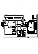
Страница 39: ... 39 SCHEMATIC DIAGRAM MAIN FRONT 1 FRONT 2 DECK FX NH2000 All manuals and user guides at all guides com ...

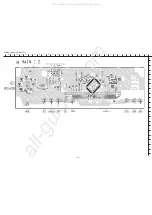
Страница 40: ...WIRING 2 DECK FX NH2000 40 10 11 12 13 14 15 16 17 18 19 20 21 22 23 24 A B C D E F G H I J K L M N O P Q R S T U 1 2 3 4 5 6 7 8 9 25 26 27 28 29 30 31 32 All manuals and user guides at all guides com ...

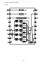
Страница 41: ... 41 IC BLOCK DIAGRAM FX NH2000 IC HA12211 IC CXA1553P All manuals and user guides at all guides com a l l g u i d e s c o m ...

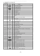
Страница 42: ...en Power is ON L under STOP status When RVS operates flashing L H repeated While REW fast flashing 24 D PAUSE O When Power is ON L under STOP status While PAUSE flashing L H repeated 25 D REC O While REC DUBBING L While REC MUTE flashing 26 D NR O When NR is ON L Not used 27 O MOTOR O When MOTOR is in operation or power on 500msec H 28 O SOL2 O When DECK 2 solenoid is in operation H 29 O SOL1 O Wh...

Страница 43: ...2 I KEY input 2 AD input 40 I KEY1 I KEY input 1 AD input 41 I MS I MS input AD input 42 I HOLD I System power supply monitor AD input Description Pin No Pin Name I O P1Ns 22 23 24 25 and 26 should be H when MX NH2000 is in DIMMER 2 mode All manuals and user guides at all guides com ...

Страница 44: ...erence level of 10kHz signal is less than 2dB 6 REC PB Sensitivity Adjustment DECK2 Settings Test tape TTA 602 NORMAL Test point TP1 Rch TP2 Lch Input signal 1kHz LINE IN Adjustment location SFR305 Lch SFR306 Rch Method Apply a 1kHz signal and REC mode Then adjust OSC attenuator so that the output level at the TP1 TP2 becomes 0dB 17mV Record and play back the 1kHz signals and adjust SFRs so that t...

Страница 45: ...IEW 1 1 FX NH2000 1 2 3 4 4 5 6 7 8 9 10 11 12 13 13 14 15 17 18 19 20 P C B P C B P C B 21 22 22 23 23 24 16 28 A B B A A A A A PLATE EARTH 2ZM 3 PLATE SHLD MECHA C C C C 26 25 27 All manuals and user guides at all guides com ...

Страница 46: ... CASS 1 21 87 NF4 217 110 HLDR LOCK 2 22 86 NF9 224 010 SPR C LOCK 23 82 NF5 229 010 PLATE LOCK 24 87 NF4 216 010 HLDR LOCK 1 25 8A SW1 016 010 PANEL SIDE L 26 8A SW1 015 010 CABI STEEL 27 8A SW1 017 010 PANEL SIDE R 28 87 A90 923 010 F BEAD 8 13 14E1314 A 87 067 703 010 BVT2 3 10 W O SLOT B 87 067 579 010 BVT2 3 8 W O SLOT C 87 B10 091 010 UTT2 3 10 W O SLOT BLK DESCRIPTION REF NO KANRI NO PART N...

Страница 47: ... 37 32 C E CUSH G DIA3 7 8 3 2 CAPSTAN N 2 2 41 7 SH 1 63 3 2 0 5 SLT SH BELT D2 2ZM3MK2 PR4N BOTTOM SIDE 2000 3 6 YPR4N HLDR IC HLDR IC 1 A A 42 16 15 14 13 12 11 10 17 7 9 19 4 6 20 5 22 21 24 23 25 26 29 29 27 28 3 2 HEAD 1 C B DECK 1 HEAD 2 C B DECK 2 PH DECK 1 RPH DECK 2 DECK 2 DECK 2 36 DECK 1 B B A 2ZM3MK2 PR4N YPR4N TOP SIDE 2000 3 6 All manuals and user guides at all guides com ...

Страница 48: ...4 010 0E LVR ASSY PINCH R2 28 82 ZM1 259 210 0E SPR T PINCH R 29 82 ZM1 240 110 0E LVR REC 30 80 ZM6 243 010 0E SH 1 75 3 6 0 5 SLT 31 82 ZM1 255 310 0E SPR E LVR DIR 32 82 ZM3 305 210 0E GEAR CAM M2 33 82 ZM1 227 310 0E LVR TRIG 34 82 ZM3 306 110 0E LVR FR M2 35 82 ZM1 265 310 0E SPR E TRIG 36 82 ZM3 339 110 0E SHAFT COUPLER N3 37 86 ZM1 206 010 0E BELT MAIN L 38 82 ZM1 322 010 0E SPR T FR 60 39 ...

Страница 49: ...5 C407 87 012 158 080 C CAP S 390P 50 CH C408 87 A11 144 080 CAP TC U 0 1 50 K B FL201 8Z SU1 605 010 FL BJ699GK L101 87 005 152 080 COIL 10UH L102 87 005 130 080 COIL 10UH L103 87 005 130 080 COIL 10UH L104 87 005 152 080 COIL 10UH L301 87 003 097 080 COIL 1UH LED201 87 A40 380 080 LED SEL6510C TP5 GRN LED202 87 A40 380 080 LED SEL6510C TP5 GRN LED203 87 A40 380 080 LED SEL6510C TP5 GRN LED204 87...

Страница 50: ... 50 TRANSISTOR ILLUSTRATION GE NH2000 E B C RN1410 All manuals and user guides at all guides com ...

Страница 51: ... GE NH2000 51 10 11 12 13 14 15 16 17 18 19 20 21 22 23 24 A B C D E F G H I J K L M N O P Q R S T U 1 2 3 4 5 6 7 8 9 25 26 27 28 29 30 31 32 All manuals and user guides at all guides com a l l g u i d e s c o m ...

Страница 52: ... 52 SCHEMATIC DIAGRAM MAIN GE NH2000 All manuals and user guides at all guides com ...

Страница 53: ... 53 FL GRID ASSIGNMENT AND ANODE CONNECTION GE NH2000 GRID ASSIGNMENT ANODE CONNECTION All manuals and user guides at all guides com ...

Страница 54: ... 54 IC BLOCK DIAGRAM GE NH2000 IC BA3835F All manuals and user guides at all guides com ...

Страница 55: ...en prologic L when not prologic 25 33 G1 G9 O FL gird output 34 40 S1 S7 O FL Segment output 41 VDD2 Connected to GND 42 VP Power FL display negative supply terminal 43 63 S8 S28 O FL Segment S8 S28 output 64 NC Not used 65 LED ON O MULTI JOG LED output 66 LED ON O MULTI JOG LED output 67 69 72 NC Not connected 70 O L FREQ ON O Spectrum analyzer low frequency output 71 O H FREQ ON O Spectrum analy...

Страница 56: ... 56 MECHANICAL EXPLODED VIEW 1 1 GE NH2000 A A A A A A 4 5 6 7 8 9 a FL 10 P C B 14 PLATE DUMMY 1 2 3 B B 11 12 B B 13 a b b All manuals and user guides at all guides com a l l g u i d e s c o m ...

Страница 57: ...T Transparent Orange GM Metallic Green YM Metallic Yellow DM Metallic Orange PT Transparent Pink 1 8Z SU1 007 010 KNOB RTRY JOG 2 8A SU1 006 010 RING JOG 3 8Z SU1 005 010 REFLECTOR JOG 4 8A SU1 004 010 WINDOW DISPLAY 5 87 CE3 023 010 BADGE AIWA 30N SILV 6 8A SU1 016 010 CABI FR YS 7 8A SU1 009 010 KEY DEMO 8 8A SU1 008 010 KEY GEQ EZ 9 8A SU1 010 010 KEY ENTER 10 88 SU1 201 110 GUIDE FL 11 8A SX1 ...

Страница 58: ...ction until click sound comes out Remove the grill frame and four pieces of rubber caps by pulling out with a flat bladed screwdriver Remove the screws from hole where installed rubber caps Insert a flat bladed screwdriver into the position indicated by the arrows and remove the panel Re move the screws of each speaker unit and then remove the speaker units TOOLS 1 Plastic head hammer 2 flat head ...

Страница 59: ...RD SPKR 2 8A SSM 005 010 PANEL FR L 3 8A SSM 001 010 PANEL FR R 4 8A SSM 004 010 PANEL TW 5 8A SSM 002 010 GRILLE FRAME ASSY 6 8Z SSM 009 010 PROTECTOR TW 7 8A SSM 602 010 SPKR W 150 8 8Z NSY 608 010 SPKR CERAMIC ASSY 9 88 SSM 603 010 SPKR TW 60 All manuals and user guides at all guides com ...

Страница 60: ...2 11 IKENOHATA 1 CHOME TAITO KU TOKYO 110 JAPAN TEL 03 3827 3111 Printed in Singapore 9620450 0251431 All manuals and user guides at all guides com ...

Отзывы: