


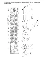


ADJUSTMENT – 1 <TUNER / FRONT>
< TUNER SECTION >
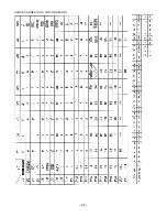
1. Clock Frequency Check
Settings :
• Test point :
TP2 (CLK)
Method :
Set to AM(MW) 1602 kHz and check that the test point
is 2052 kHz ± 45 Hz.
2. AM(MW) VT Check
Settings :
• Test point :
TP1 (VT)
Method :
Set to AM(MW) 1602 kHz and check that the test point
is less than 8.0 V. Then set to AM(MW) 531 kHz and
check that the test point is more than 0.6 V.
3. LW VT Adjustment<EZ, K>
Settings :
• Test point :
TP1 (VT)
• Adjustment location : L942
Method :
Set to LW 144 kHz and adjust L942 so that the test point
becomes 1.3 V ± 0.05 V. Then set to LW 290 kHz and
check that the test point is less than 8.0 V.
4. AM(MW) Tracking Adjustment
Settings :
• Test point :
TP8 (Lch), TP9 (Rch)
• Adjustment location : L951(1/3)
Method :
Set to AM(MW) 999 kHz and adjust L951(1/3) so that
the test point becomes maximum.
5. LW Tracking Adjustment<EZ, K>
Settings :
• Test point :
TP8 (Lch), TP9 (Rch)
• Adjustment location :
L941 ................................................... 144 kHz
TC942 ................................................. 290 kHz
Method :
Set up TC942 to center before adjustment.
The level at 144 kHz is adjusted to maximum by L941.
Then the level at 290 kHz is adjusted to maximum by
TC942.
6. AM IF Adjustment
Settings :
• Test point :
TP8 (Lch), TP9 (Rch)
• Adjustment location :
L802 ................................................... 450 kHz
7. FM VT Check<EZ, K>
Settings :
• Test point :
TP1 (VT)
Method :
Set to FM 87.5 MHz check that the test point is more
than 0.5 V. Then set to FM 108.0 MHz and check that
the test point is less than 8.0 V.
8. FM VT Check<V>
Settings :
• Test point :
TP1 (VT)
Method :
Set to FM 65.0 MHz check that the test point is more
than 1.0 V. Then set to FM 108.0 MHz and check that
the test point is less than 9.5 V.
9. FM Tracking Check
Settings :
• Test point :
TP8 (Lch), TP9 (Rch)
Method :
Set to FM 98.0 MHz and check that the test point
is less than 13 dBµV<EZ, K>, 8 dBµV<V>.
10. DC Balance / Mono Distortion Adjustment
Settings :
• Test point :
TP3, TP4 (DC Balance)
TP8 (Lch), TP9 (Rch)
(Mono Distortion)
• Adjustment location : L801
• Input level :
60 dBµV
Method :
Set to FM 98.0 MHz and adjust L801 so that the voltage
between TP3 and TP4 becomes 0 V ± 500 mV with
minimum distortion.
11. Output Level Check
<AM(MW)>
Settings :
• Test point :
TP8 (Lch), TP9 (Rch)
• Input level : 74 dBµV
Method :
Set to AM(MW) 999 kHz and check that the test point
is 50 mV ± 3 dB.
<FM>
Settings :
• Test point :
TP8 (Lch), TP9 (Rch)
• Input level : 60 dBµV
Method :
Set to FM 98.0MHz and check that the test point is
150 mV ± 3 dB.
12. FM Separation Check
Settings :
• Test point :
TP8 (Lch), TP9 (Rch)
• Input level :
60 dBµV
Method :
EZ,K: Set to FM 83.0 MHz and check that the
separation is more than 12 dB.
V: Set to FM 98.0 MHz and check that the separation
is more than 25 dB.
< FRONT SECTION >
13. µ-CON OSC Adjustment
Settings :
• Test point :
TP5 (K-SCAN)
TP6 (GND)
• Adjustment location : L501
Method :
Insert AC plug while pressing of "POWER" key and
"TUNER" function key.
Connect a frequency counter across TP5 and TP6.
Then adjust L501 so that the test point becomes
92.470 Hz ± 0.092 Hz.
[ Manual Reset ]
Make up for RESET after adjustment.
* Reset is to press "POWER" key while pressing of
"CLEAR (STOP)" key.
– 30 –
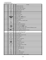
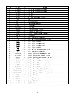
Содержание NSX-AJ200U
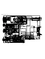
Страница 11: ... 11 SCHEMATIC DIAGRAM 1 MAIN 1 2 EZ K ...
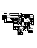
Страница 12: ...SCHEMATIC DIAGRAM 2 FRONT DECK EZ K 12 ...
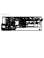
Страница 13: ...SCHEMATIC DIAGRAM 3 TUNER EZ K 13 ...
Страница 14: ...SCHEMATIC DIAGRAM 4 MAIN 2 2 PT SECTION 201K 207EZ 14 ...
Страница 16: ...SCHEMATIC DIAGRAM 5 MAIN 1 2 V 16 ...
Страница 17: ...SCHEMATIC DIAGRAM 6 FRONT DECK V 17 ...
Страница 18: ...SCHEMATIC DIAGRAM 7 TUNER V 18 ...
Страница 19: ...SCHEMATIC DIAGRAM 8 MAIN 2 2 PT SECTION 203EZ 203V 19 ...
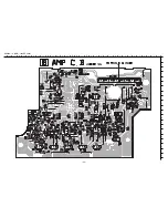
Страница 21: ...SCHEMATIC DIAGRAM 9 AMP 201K 207EZ 21 ...
Страница 23: ...SCHEMATIC DIAGRAM 10 AMP 203EZ 203V 23 ...
Страница 25: ...IC BLOCK DIAGRAM 25 ...
Страница 26: ...FL HNA 10SS19T GRID ASSIGNMENT ANODE CONNECTION PIN CONNECTION 26 GRID ASSIGNMENT ...
Страница 27: ... 27 ANODE CONNECTION PIN CONNECTON ...
Страница 39: ...2 11 IKENOHATA 1 CHOME TAITO KU TOKYO 110 JAPAN TEL 03 3827 3111 Printed in Singapore 9820572 0251431 ...


