background image

MECHANICAL ADJUSTMENTS

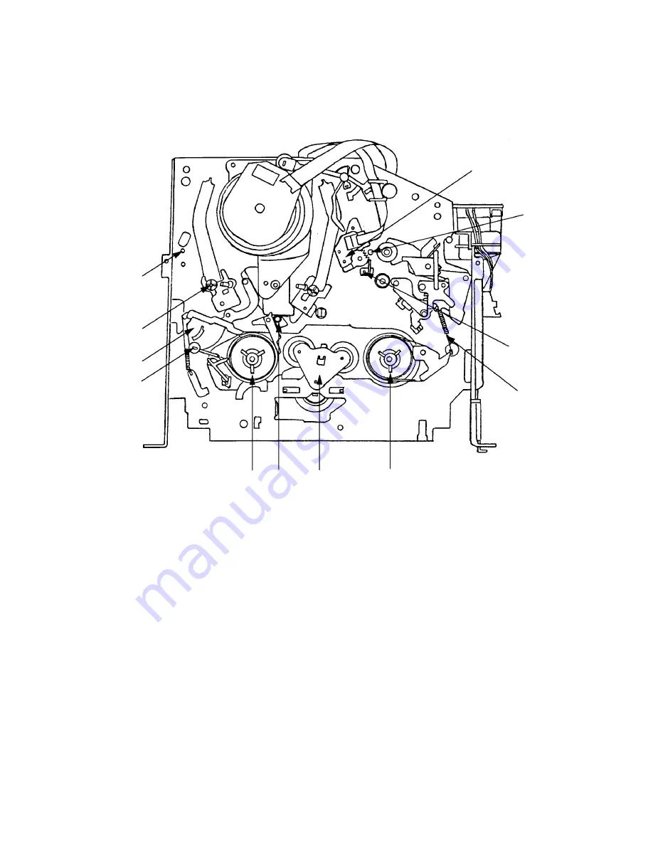
3. MECHANISM ADJUSTMENT PARTS LOCATION GUIDE

1

2

3

4

5

6

7

8

9

11

10

12

7.
8.
9.

10.
11.
12.

P4 Post
T Brake Spring
T Reel Ass'y
Idler Ass'y
S-S Brake Spring
S Reel

1. Tension Adjust
2. Tension Arm
3. Guide Roller
4. P1 Post
5. Audio/Control Head
6. X value adjustment driver hole

D1-4

Содержание HV-FX5100

Страница 1: ... SP 5 hours with E 300 tape LP 10 hours with E 300 tape NTSC playback only SP 3 hours 30 minutes with T 210 tape 1 0 Vp p 75 ohm unbalanced 1 0 Vp p 75 ohm unbalanced 53 dB nominal SCART 3 8 dBs 50 Kohm RCA 3 8 dBs 50 Kohm SCART 3 8 dBs less than 1 Kohm RCA 3 8 dBs less than 1 Kohm 3 tracks Hi Fi sound 2 tracks Normal sound 1 track HI FI WOW AND FLUTTER TAPE SPEED RECORDING PLAYBACK TIME VIDEO INP...

Страница 2: ...S Y C AUDIO HEAD AMP SYSTEM CONTROL SERVO TIMER TUNER HIFI 21PIN OSD VPS NICAM OPERATION POWER DECK SCHEMATIC DIAGRAM OPERATION SCHEMATIC DIAGRAM PRINTED CIRCUIT BOARDS OPERATION 1 2 DECK PRINTED CIRCUIT BOARDS SYSCON Y C AUDIO HEAD AMP SCHEMATIC DIAGRAM SYSTEM CONTROL SERVO TIMER SCHEMATIC DIAGRAM 21PIN OSD VPS SCHEMATIC DIAGRAM TUNER HIFI SCHEMATIC DIAGRAM POWER SCHEMATIC DIAGRAM DISPLAY SCHEMAT...

Страница 3: ...e wiring is designed not to get closer to the pyrogenic parts and high voltage parts Therefore put these parts in the original positions PERFORM A SAFETY CHECK AFTER SERVICING 4 Confirm that the screws parts and wiring which were removed in order to service are put in the original positions or whether there are the portions which are deteriorated around the serviced places serviced or not Check th...

Страница 4: ...o Fig 1 2 1 2 Open Flap to 90 and flex in direction of arrow A at the same time slide in direction of arrow B Then lift in direction of arrow C A C B Flap Fig 1 2 1 1 1 A 2 2 2 2 Operation 1 PCB 3 3 3 B 2 2 2 4 4 4 4 Operation 2 PCB Front Cabinet 1 3 DECK CHASSIS Refer to Fig 1 3 Remove the 3 screws 1 Remove the screw 2 Disconnect the following connectors CP1001 CP1002 CP1004 CP4001 CP4002 and CP4...

Страница 5: ...CASSETTE SIDE L R Refer to Fig 2 5 Remove the Locker Spring Unlock the 4 supports 1 and then remove the Cassette Side L R 1 2 NOTE When you install the Cassette Side L R be sure to move the Locker L R after installing Locker Spring Cassette Side L Cassette Side R 1 1 1 Locker L Locker R 1 Fig 2 5 Screw Torque 5 0 5kgf cm DECK COVER FLAP LEVER TAPE GUIDE R Refer to Fig 2 2 Move the Cassette Holder ...

Страница 6: ...ion Adjust Unlock the 2 supports 3 and remove the Tension Band Ass y Unlock the support 4 and remove the Tension Holder 1 2 3 4 5 6 7 Tension Holder 4 2 Tension Adjust Tension Band Ass y Tension Arm Ass y 1 Tension Spring Inclined S Ass y Fig 2 9 A NOTE When you install the Tension Adjust install as shown in Fig 2 9 B Refer to Fig 2 9 B Adjust the direction of the Marker to inside Fig 2 9 B 2 10 T...

Страница 7: ...AD Refer to Fig 2 13 A Remove the screw 1 Remove the A C Head Base Remove the 3 screws 2 Remove the A C Head and A C Head Spring 1 2 3 4 NOTE Do not touch the A C Head Use gloves When you install the A C Head Spring install as shown in Fig 2 13 B Refer to Fig 2 13 B When you install the A C Head tighten the screw 1 first then tighten the screw 2 finally tighten the screw 3 1 2 3 A C Head 2 2 A C H...

Страница 8: ...ASS Y Refer to Fig 2 15 Unlock the support 1 and remove the AHC Ass y Remove the 3 screws 2 Remove the Cylinder Unit Ass y 1 2 3 When you install the Cylinder Unit Ass y tighten the screws from 1 to 3 in order while pulling the Ass y toward the left front direction NOTE 2 3 2 1 2 2 Cylinder Unit Ass y 1 AHC Ass y Screw Torque 5 0 5kgf cm Fig 2 15 2 16 CAPSTAN DD UNIT Refer to Fig 2 16 Remove the C...

Страница 9: ... Arm T Ass y Loading Gear S LED Reflecter Fig 2 19 A NOTE When you install the Loading Arm S Ass y Loading Arm T Ass y and Main Loading Gear align each marker Refer to Fig 2 19 B Loading Arm T Ass y Main Loading Gear Marker Marker Loading Arm S Ass y Fig 2 19 B 4 Loading Arm S Ass y Loading Gear Spring Loading Gear Spring 2 20 INCLINED S T ASS Y Refer to Fig 2 20 Unlock the support 1 and remove th...

Страница 10: ...lop Frequency Generator Front Loading Switch Frequency Modulation Frequency Sub Carrier Forward Generator Ground High Pass Filter I K L M N O P R S H SW Hz IC IF IND INV KIL L LED LIMIT AMP LM LDM LP L P F LUMI M MAX MINI MIX MM MOD MPX MS SW NC NR OSC OPE PB PB CTL PB C PB Y PCB P CON PD PG P P R REC REC C REC Y REEL BRK REEL S REF REG REW REV RVS RF RMC RY S CLK S COM S DATA SEG SEL SENS SER SI ...

Страница 11: ...tor Separation Transistor Tracking Trick Playback Test Point Unregulated Volt Voltage Controlled Oscillator Video Intermediate Frequency Vertical Pulse Voltage Display Video Playback Variable Resistor Video Recording Visual Search Fast Forward Visual Search Rewind Voltage Super Source Vertical Synchronization Voltage Tuning Crystal Luminance Chrominance C1 2 ...

Страница 12: ... to the center position Refer to the MECHANICAL ADJUSTMENT GUIDE ROLLER and ELECTRICAL ADJUSTMENT PG SHIFTER Press the ATR button on the remote control for more than 2 seconds during PLAY Press both STOP button and CH UP button on the set for more than 2 seconds during PLAY Press both FF button and CH UP button on the set for more than 2 seconds Adjust the PG SHIFTER automatically Refer to the ELE...

Страница 13: ... those parts in contact with the tape Clean the rubber and parts which the rubber touches Replace when rolling becomes abnormal Clean the Head CONFIRMATION OF USING HOURS PLAY REC total hours can be checked on the FIP Total hours are displayed in 16 system of notation 1 2 3 4 Press both FF button and CH UP button on the set for more than 2 seconds Adjust the ADDRESS to FD by SET button and read th...

Страница 14: ...ally Clean the full erase head in the same manner Refer to the figure below Audio Control Head 2 TAPE RUNNING SYSTEM When cleaning the tape transport system use the gauze moistened with isopropyl alcohol 3 CYLINDER Wrap a piece of chamois around your finger Dip it in isopropyl alcohol Hold it to the cylinder head softly Turn the cylinder head counterclockwise to clean it in the direction of the ar...

Страница 15: ...6 E9 15 F3 41 3 4 5 6 7 8 The unit will now have the correct DATA for the new MEMORY IC ADDRESS DATA 1 2 Turn on the POWER and press both FF key and CH UP key on the set for more than 2 seconds ADDRESS and DATA should appear as FIG 1 Fig 1 ADDRESS is now selected and should blink Using the SET or keys on the remote step through the ADDRESS until required ADDRESS to be changed is reached Press ENTE...

Страница 16: ...speed model JG001C Stair Steps 7KHz For 2 speed model JG001D Color Bar 1KHz For 2 speed model JG001V X Value Adjustment For 2 speed model JG002B VSR Torque Brake Torque S Reel T Reel Ass y JG002E Brake Torque T Reel Ass y JG002F VSR Torque Brake Torque S Reel JG005 Guide Roller Adjustment JG153 X Value Adjustment JG022 JG024A Reel Disk Height Adjustment Used to connect the test point of SERVICE an...

Страница 17: ...erve the chroma signal There are two types of the new alignment tape CH 1B for NTSC and CH 2 for PAL On each tape four signals 1 4 are recorded for the times and in the order shown below The TTV MP1 for M PAL TTV MS1 for MESECAM and TTV S1 for SECAM alignment tapes have the same contents as the previous tapes 1 8min 2 2min 3 5min 4 5min Method Contents 1 Model Model Contents 1 Application Now in u...

Страница 18: ...a video tape E 180 recorded in standard speed mode Set the unit to the PLAY mode Install the tentelometer as shown in Fig 1 3 Confirm that the meter indicates 20 2gf in the beginning of playback 1 2 USING A CASSETTE TYPE TORQUE TAPE JG100A 1 2 3 After confirmation and adjustment of Tension Post position Refer to item 1 2 load the cassette type torque tape JG100A and set to the PLAY mode Confirm th...

Страница 19: ...Spring 2 CONFIRMATION AND ADJUSTMENT OF TAPE RUNNING MECHANISM Tape Running Mechanism is adjusted precisely at the factory Adjustment is not necessary as usual When you replace the parts of the tape running mechanism because of long term usage or failure the confirmation and adjustment are necessary 2 1 GUIDE ROLLER Playback the VHS Alignment Tape JG001C or JG001E Refer to SERVICING FIXTURE AND TO...

Страница 20: ...distortion is appeared then adjust the a Reflected picture of Stamp Mark Stamp Mark Audio Control Head P4 Post Fig 2 2 A Audio Control Head 1 3 2 Fig 2 2 B Tape Audio Control Head Fig 2 2 C 0 25 0 05mm TAPE RUNNING ADJUSTMENT X VALUE ADJUSTMENT Confirm and adjust the height of the Reel Disk Refer to item 1 1 Confirm and adjust the position of the Tension Post Refer to item 1 2 Adjust the Guide Rol...

Страница 21: ...ARTS LOCATION GUIDE 1 2 3 4 5 6 7 8 9 11 10 12 7 8 9 10 11 12 P4 Post T Brake Spring T Reel Ass y Idler Ass y S S Brake Spring S Reel 1 Tension Adjust 2 Tension Arm 3 Guide Roller 4 P1 Post 5 Audio Control Head 6 X value adjustment driver hole D1 4 ...

Страница 22: ... 19 of J4501 Playback the alignment tape JG001C Press and hold the Tracking Auto button on the remote control more than 2 seconds to set tracking to center Press both CH UP button and STOP button on the set for more than 2 seconds If the indicator ATR disappear s the adjustment is finished Refer to Fig 1 1 A B 6 5H CH 1 CH 2 CH 1 CH 2 6 5H Fig 1 1 A Fig 1 1 B Read and perform this adjustment when ...

Страница 23: ...ELECTRICAL ADJUSTMENTS 2 ELECTRICAL ADJUSTMENT PARTS LOCATION GUIDE SYSCON PCB T501 J4501 TP4002 TP4001 TU6001 TP1002 TP1001 D2 2 ...

Страница 24: ...N Does DISPLAY light Is F501 broken Check the peripheral circuit to pin 14 of T501 Check IC1002 Replace Q510 No No Yes Yes Replace Q502 Is the voltage at pin 20 of IC1002 about 5V Is the voltage at base of Q502 about 5V Is the voltage at collector of Q507 about 5 6V TROUBLESHOOTING GUIDE E 1 ...

Страница 25: ...sert a cassette and press PLAY button Yes No Yes No Check REEL SENSOR and BELT CAPSTAN Does it Power off in about 3 seconds Check POWER BLOCK Does it Power off in about 6 seconds Check TAPE LOADING LOADING BELT DD MOTOR and CYLINDER MOTOR E 2 ...

Страница 26: ...ROTATING DURING PLAYBACK AND RECORDING No No Yes Yes Check AT 12 6V line of POWER BLOCK Is the voltage at pin 2 of CP1002 about DC11 25V In playback is the voltage at pin 5 of CP1002 about DC1 52V Replace CYLINDER MOTOR Check IC1002 E 3 ...

Страница 27: ... Check AUDIO BLOCK Yes No Replace CAPSTAN DD UNIT Check IC1002 Yes No Is AUDIO HEAD scratched In playback is the voltage at pin 4 of CP1003 2 6V AUDIO SHAKES Replace AUDIO HEAD Is input level at pin 85 of IC1002 about 0 4Vp p E 4 ...

Страница 28: ... cassette is inserted is the voltage between pins 3 and 4 of CP1004 about 9 8V When a cassette is inserted is the voltage at pin 47 of IC1002 5V Does WORM GEAR on CASSETTE LOADING BLOCK activate Check FRONT LOADING GEARS and LOCKER Check LED and PHOTO SENSOR on SYSCON PCB Replace LOADING MOTOR Replace IC1002 Check circuit of CASSETTE LOADING BLOCK E 5 ...

Страница 29: ...NG CASSETTE IT EJECTS IMMEDIATELY No Yes No Yes Check IC1002 Does another cassette go down When cassette is inserted is the voltage at pins 4 and 3 of IC1002 0V Check FRONT LOADING GEARS Defective CASSETTE or CASSETTE LOADING BLOCK E 6 ...

Страница 30: ...TROUBLESHOOTING GUIDE Yes No Check DECK MECHANISM Is the voltage changing at pin 11 of IC1002 when you press FF REW FF REW DO NOT WORK Check pins 9 and 10 of IC1002 lines E 7 ...

Страница 31: ...V Check Power circuit No No Yes Yes No Yes No No Yes Yes Is the voltage at pin 2 of CP1002 AT 12 6V Does TP4001 feed HEAD SWITCHING PULSE signal TAPE LOADING IS OK BUT UNLOADS IMMEDIATELY Replace CYLINDER UNIT Check REEL SENSOR Replace IC1002 Does PG PULSE signal appear at pin 86 of IC1002 E 8 ...

Страница 32: ...ge at pin 5 of CP1002 1 5V No Yes Yes Is FG output level at pin 3 of CP1002 about 4 0Vp p No Replace CYLINDER MOTOR Is the voltage at pin 5 of CP1002 1 5V Is FG output level at pin 3 of CP1002 about 4 0Vp p PLAYBACK PICTURE JITTERS HORIZONTALLY Replace CYLINDER MOTOR Replace IC1002 PLAYBACK PICTURE SHAKES E 9 ...

Страница 33: ...IC1002 Check CONTROL HEAD No Yes No Yes No Yes By manual tracking does the DC level at pin 84 of IC4001 change In auto tracking is the voltage at pin 6 of IC1002 more than DC 1V Check CYLINDER UNIT Does the CTL PULSE about 4 6Vp p appear at pin 97 of IC1002 E 10 ...

Страница 34: ...e WHEN IN PLAYBACK FAST FORWARD OR REWIND MODE IS ACTIVATED UNIT STOPS IMMEDIATELY No Yes No Yes Replace IC1002 Does the REEL SENSOR PULSE signal appear at pins 79 and 80 IC1002 Check Q1001 and Q1002 Refer to section CAPSTAN DD MOTOR NOT ROTATING E 11 ...

Страница 35: ...noise disappear in the picture PLAYBACK PICTURE JITTERS VERTICALLY Does tracking noise appear in the picture Check P B ENVELOPE Are GUIDE POSTS the right height Adjust GUIDE POST height Is PG SHIFTER adjustment 6 5H Yes Yes Is PB Y waveform normal Check PB Y circuit Replace IC1002 No Yes Yes No No No E 12 ...

Страница 36: ... E E appearing on the Monitor TV No Is the voltage at pins12 36 61 and 90 96 of IC4001 5V Check Power circuit Check connection of the CYLINDER Replace IC4001 Check VIDEO OUT LINE and IC4001 Is there FM signal at pins 78 and 79 of IC4001 Is there VIDEO signal at pin 52 of IC4001 E 13 ...

Страница 37: ...TROUBLESHOOTING GUIDE Check Q4802 circuit No Yes Does COMPOSITE signal appear at pin 52 of IC4001 NO COLOR DURING PLAYBACK Replace IC4001 E 14 ...

Страница 38: ...URE IS NOISY EVEN AFTER CLEANING HEADS No Yes No Yes Check CYLINDER UNIT Is FM signal at pin 79 of IC4001 270mVp p No Yes Is VIDEO output at the emitter of Q4802 2Vp p and are there any noises Replace J4501 Check IC4001 and Q4802 E 15 Perform the interchangeable adjustment of DECK ...

Страница 39: ...DE Replace J4501 Check VIDEO input circuit No Yes Yes NO COLOR DURING SELF RECORDING AND PLAYBACK Does VIDEO signal appear at pin 31 of IC4001 No Does color signal at pin 52 of IC4001 Check Q4802 EMITTER Check IC4001 E 16 ...

Страница 40: ...s No Yes Replace IC4001 Does AUDIO signal appear at pin 11 of IC4001 1Vp p Does audio appear on E E Refer to section NO E E Does AUDIO signal appear at pin 2 of IC4001 6mVp p Check AUDIO HEAD for debris or stains Check the connector from AUDIO HEAD is fully inserted into CP4002 Replace IC4001 E 17 ...

Страница 41: ... In playback check the voltage at pin 3 of CP1003 is 2V or at pin 62 of IC1002 is 2 5V CAPSTAN DD MOTOR NOT ROTATING In playback is the voltage at pin 5 of CP1003 12V Check POWER circuit Is the voltage at pin 8 of CP1003 5V Check pins 77 78 of IC1002 and peripheral circuit In playback is the voltage at pin 4 of CP1003 2 5V E 18 ...

Страница 42: ...IO signal at pin 11 of IC4001 No Yes Is BIAS level O K at L4005 Is the voltage at pin 2 of L4005 5 8V Check POWER circuit Is the voltage at pin 29 of IC1002 about 5V Is there AUDIO signal at pin 5 of CP4002 Check the circuit between pin4 of IC4001 to pin 5 of CP4002 Replace IC4001 Check the lead wire and connector to A C HEAD E 19 ...

Страница 43: ...DE No Check IC1002 Does mode indicator appear in Display Check Operation PCB Yes Yes No CASSETTE IN AND DOWN UNIT HAS NO FUNCTIONS Does VCR operate with the remote control Check LOADING MOTOR and the peripheral parts E 20 ...

Страница 44: ...EO RECORDED FROM INPUT JACK OR TUNER Yes No No Yes Does the VIDEO signal appear at pin 52 of IC4001 Does VIDEO signal appear at pin 31 of IC4001 Check the circuit from VIDEO input jack to IC4001 from Tuner Pack to IC4001 Replace IC4001 Check CYLINDER UNIT E 21 ...

Страница 45: ...gnal appear at pin 24 of TU6001 Disconnect the plugs from the VIDEO AUDIO input jacks Are the plugs connected to the VIDEO AUDIO input jacks Does AUDIO signal appear at pin 21 of TU6001 No Yes Is there VIDEO waveform at pin 52 of IC4001 Check IC4501 Does AUDIO signal appear at pin 1 and 2 of IC6601 Do the voltages appear at each terminal PB 5V TU 32V and B 5V of TU6001 Check Power Block Replace Q6...

Страница 46: ...s AUDIO signal appear at pins 6 and 7 of IC5501 Does AUDIO signal appear at pin 21 of IC5501 Does AUDIO signal appear at pin 22 of IC5501 Does AUDIO signal appear at pins 15 and 18 of IC5501 Check POWER BLOCK Check J4501 and peripheral circuit NO E E AUDIO MONO Is the voltage at pin 40 of IC5501 5V Replace IC5501 Check J4501 and peripheral circuit E 23 ...

Страница 47: ...TROUBLESHOOTING GUIDE Yes No NO E E AUDIO STEREO Check the circuit between IC5501 to J4501 Does audio appear on E E Refer to section NO E E AUDIO MONO E 24 ...

Страница 48: ...IO MONO No No No No NO TUNER AUDIO MONO Does AUDIO signal appear at pins 1 and 2 of IC6601 Does AUDIO signal appear at pins 15 and 18 of IC5501 Check J4501 and peripheral circuit Replace IC6601 Does audio appear on E E Does AUDIO signal appear at pin 38 of IC6601 Yes Yes Yes Yes E 25 ...

Страница 49: ...TROUBLESHOOTING GUIDE No Yes NO TUNER AUDIO STEREO Does signal appear at pin 25 of IC6601 Refer to section NO TUNER AUDIO MONO Reploce TU6001 E 26 ...

Страница 50: ...O Hi Fi No Yes No Yes Yes Is the voltage at pin 44 of IC5501 high No Does audio appear on E E Does audio appear on PB Replace IC5501 Refer to section NO E E AUDIO STEREO Refer to section NO NORMAL AUDIO ON PLAYBACK Replace IC1002 E 27 ...

Страница 51: ...TROUBLESHOOTING GUIDE Hi Fi AUDIO CANNOT BE RECORDED Does audio appear on E E Refer to section NO E E AUDIO MONO No Yes No Yes Is the voltage at pin 44 of IC5501 hight Replace IC5501 Replace IC1002 E 28 ...

Страница 52: ...NC O Not used 22 SENS LED O Mecha state sensor LED 23 NC O Not used 24 NC O Not used 25 FF REW L O Output L when fast forwarding or rewinding 26 CAP MID H O Power of Capstan Motor select 27 CAP HI H O Power of Capstan Motor select 28 HEATER SW O 30V ON OFF Control 29 NA REC H O Control the Bias OSC for audio head 30 VV H O Not used 31 SERVICE 1 I Setting of service mode 1 32 SP STILL H O Not used ...

Страница 53: ...2K MONI O Output 32 768KHz monitor 16 384KHz output to check the clock 74 Hi Fi MUTE O Control the Hi Fi IC 75 V REC ST O Control the Head Amp for video and Hi Fi audio 76 PICTURE CTL O Output pulse to control the Y C IC for sharpness 77 CAP CTL O Output servo of the capstan motor 78 CYL CTL O Output L when fast forwarding or rewinding 79 REEL S I Input terminal of reel sensor supply 80 REEL T I I...

Страница 54: ...SERVO TIMING CHART IC1001 OEC7035A DPG 6 PIN DFG 7 PIN H SW P 8 PIN CH 1 CH 2 V SYNC E E 4 PIN REC CTL REC 7 PIN V SYNC TRICK PB 3 PIN WAVEFORM CHANGES DEPENDED ON THE TAPE SPEED G 1 ...

Страница 55: ...G CLUTCH DIRECT CONNECTION PINCH ROLLER LOADING DIRECTION FWD CAPSTAN FWD ROTATING DIRECTION CAPSTAN RVS ROTATING DIRECTION LIGHT RECEIVING LIGHT RECEIVING H LIGHT GUARD LIGHT RECEIVING LIGHT GUARD LIGHT GUARD L STP FF FWD T BRAKE S BRAKE TAPE IN POWER OFF FF REW STP CASSETTE DOWN FWD TAPE LOADING FWD WHEN MSSEN A IS CHANGED FROM LIGHT GUARD TO LIGHT RECEIVING CASSETTE IN WILL BE DETECTED FWD RVS ...

Страница 56: ...TZJ4 7B T 77 IC 44PIN 30PIN 8PIN 3PIN 8PIN 5PIN BU2979K LC74775M M24C08 BN6 NJM431L BA6955AN STR F6552 TDA9605H 36PIN RE5VS31A TDA9874H LA7158M 100PIN HA118217F OEC7035A TRANSISTOR 2SB926 S T AA 2SA1037AKT146R S GP1S94L DTA124EKAT146 DTA143ESTP GP1S566 2SC2274K E F AA 2SC2412KT146 R S DTC114EKAT146 2SD734 E F AA DTC124EKAT146 DTC143EKAT146 DTC144EKAT146 CATHODE ANODE CATHODE ANODE 1 1 1 1 2 3 1 1 ...

Страница 57: ...O SLPF MAIN DE EMPH P R LPF 31 26 19 23 21 24 18 YLPF P R P R CLAMP NL EMPH NL DE EMPH FBC ALC CLAMP LPF YNR ATT P R N C D E Y APA VIDEO AGC SQUELCH FBC VIDEO ALC CLEAR SYNC 6db AMP 6db AMP C SQUELCH C K N P B D BPF MIX LEVELADJ B E C K P R P R P R P R VCA DELAY CLPF CCD LPF MAIN CONV1 MAIN CONV2 CLPF P R 60 58 55 54 52 35 46 C CCD 42 Y CCD 39 P R Y C AUDIO CCD H AMP IC4001 HA118217F 4 5 SP CH2 L ...

Страница 58: ... BOT 14 7 8 LDM FWD LDM RVS REMOCON KEY A CH UP OTP 53 72 71 OTP IIC DATA IIC CLK 6 18 V ENV V H SW 29 NA REC H EEP ROM IC1099 M24C08 BN6 6 5 70 63 CG CLK CG CS 68 CG DATA IIC DATA IIC CLK ENV DET Y C AUDIO HAED AMP V H SW NA REC H IIC DATA IIC CLK CG CLK TUNER HIFI 21PIN OSD VPS NICAM CG CS CG DATA 5 3 2 CYL DRIVE CYL FG CYL B CP1002 MICRO MOTOR 78 87 86 1 CYL PG Q1008 CYL VCO SW D1001 AT12 6V P ...

Страница 59: ...16 18 19 CLAMP CLAMP CLAMP CLAMP 4 TU6001 24 Q6003 BUFFER 2 6 22 3 5 11 12 21 2 J4204 3 37 35 36 21 22 44 NICAM IC6601 TDA9874H 1 2 38 13 25 HIFI ENV DET HF1 HF COM HF2 A V SW IC IC4501 LA7158M Q4801 DC CLAMP I 3 42 43 I C DATA DECODER 2 BPF 1 3M 1 4M BPF 1 7M 1 8M HF LPF HF LPF PPL 1 3M 1 4M CCO PPL 1 7M 1 8M CCO 2 3 6 7 9 17 8 19 16 20 DECODER SELECT OUTPUT SELECT INPUT SWITCH OUTPUT LINE SELECT...

Страница 60: ...Q601 POWER OTP SYSCON SERVO TIMER REMOCON KEY A PHOTO COUPLER T501 IC502 NJM431L VOLTAGE CTL 1 2 Q501 3 18 L503 AC IN F501 14 11 D502 D505 12 17 SW REG IC501 STR F6552 RECTIFIER HEATER SW Q505 HEATER ON SW Q503 CAP VCO SW Q508 CAP SW Q509 CAP VCO P CON 5V SW Q507 P ON SW Q502 AT 5 8V CAP HI H POWER ON H POWER FAIL OPERATION HEATER SW SYSCON SERVO TIMER HEATER_DC HEATER_DC D525 19 21 14 17 4 1 P ON...

Страница 61: ...TAGE AT EACH PART WAS OF PRINTING AND SUBJECT TO CHANGE WITHOUT NOTICE NOTE THIS SCHEMATIC DIAGRAM IS THE LATEST AT THE TIME CP102 CP1001 173979 2 1 2 S102 S101 S104 S103 S106 S105 Q102 RPT 38PB113 EOT SENSOR Q101 RPT 38PB113 BOT SENSOR CP101 CP1004 52044 0445 1 2 3 4 J 1 FROM TO SYSCON SERVO TIMER FROM TO SYSCON SERVO TIMER DECK PCB DECK SCHEMATIC DIAGRAM M101 0 5 1 EOT VCC PCB550 VE8851 LOADING ...

Страница 62: ...10 OTPB SW609 SKQNAED010 POWER D601 SLZ 345B 02 T1 OTPB CD602 CP652 CH25082A 1 2 3 4 5 OF PRINTING AND SUBJECT TO CHANGE WITHOUT NOTICE NOTE THIS SCHEMATIC DIAGRAM IS THE LATEST AT THE TIME CAUTION DIGITAL TRANSISTOR DURING PLAYBACK MEASURED WITH THE DIGITAL TESTER NOTE THE DC VOLTAGE AT EACH PART WAS Q601 DTA143ES OTPB SW C601 470P B CAUTION DIGITAL TRANSISTOR CD601 CP651 CH23042A 1 2 3 J 2 TO DI...

Страница 63: ...1 Q101 Q102 CP102 PRINTED CIRCUIT BOARDS OPERATION 1 OPERATION 2 DECK SW605 SW604 SW601 SW603 SW602 SW606 CD601 R601 R603 R602 R604 R605 R606 SW608 SW607 SW610 SW609 D601 Q601 C601 R609 R608 CD602 R607 J 3 ...

Страница 64: ...8 C6613 C6616 C6617 R6611 R6609 R6614 R6606 C6607 I C 5 5 0 1 C4047 C4011 C4016 C4014 C4020 C6621 C6603 R1041 R1039 C1017 Q4501 R6005 Q1003 R1019 R1073 R1054 C1020 R1050 C1018 R5510 R5512 C5521 C5526 C5525 R5509 R5504 R5503 C5508 C5506 C5501 R5502 C5507 R5516 C5512 C5515 C5516 C5510 C4049 C4051 R4025 C4071 C4076 R4045 C4080 C4082 R1006 R1061 C1037 C1030 C1024 C1035 C1040 C1031 Q1006 Q1007 R1057 C4...

Страница 65: ...029 C1023 W070 W071 W072 W073 L4015 L4013 C4073 C4061 L4011 C4041 C4043 W074 W075 W076 W078 W079 W082 W083 W084 W085 W086 W087 W088 W089 W091 W092 W095 CP651_1 W098 W099 W100 W101 R4034 TP1002 TP1003 TP1001 W103 W842 W832 R5506 R5507 L6601 L6602 R6602 W104 W105 TP4001 TP4002 W106 W107 W108 W109 W110 W111 C4068 W113 W114 J4501 W115 W116 W117 W118 W119 W120 W121 W122 W123 W125 W126 R4803 W127 R1033 ...

Страница 66: ...4 C4042 C4039 C4033 C4044 IC1001 C1007 D517_1 C516 C1006 R4512 J4204 C4079 C4075 W007 W008 C4084 C4090 L4009 C4077 L4012 W009 W010 X1002 R4507 W011 TU6001 C4539 L4505 C4547 L4503 L4510 L4507 L4508 L4502 L4501 L4504 L4509 L4506 C4553 C4546 W015 W016 W017 W018 C4530 W025 R4516 W026 W027 W028 C4081 Q4004 L4003 C4010 C4024 R4017 W801 R4007 W031 R4046 R4028 Q4007 Q4006 C4059 R4818 L4807 W849 C4820 L480...

Страница 67: ...LAYBACK LUMINANCE SIGNAL PLAYBACK COLOR SIGNAL AUDIO SIGNAL REC AUDIO SIGNAL PB 2FSC IIC_DATA IIC_CLK P CON 5V VV H V H_SW EE VV_V_OUT DUMMY_V SYNC PICTURE_CTL NA_REC H DUMMY_V SYNC SYNC A_MUTE TRICK H IIC_DATA IIC_CLK ENV DET CTL CTL 2FSC V H_SW SYNC SWD_VIDEO_IN EE VV_V_OUT ENV DET SP L SP_COM NORMAL_A_IN NORMAL_A_OUT SP R HF1 P CON 5V HF2 HF_COM EP L EP_COM AT 5 8V EP R P CON 5V P CON 5V GND P ...

Страница 68: ...C_MUTE HIFI_ENV DET HIFI_H SW VV H IIC_CLK IIC_DATA AGC_DET AFT_S_CURVE IIC_CLK IIC_DATA CG_CS CG_CLK PERI_CTL L CG_DATA RGB_ON H AT 5V POWER_FAIL POWER_FAIL CAP_VCO AT 5V A AT 5 8V POWER_ON H AT 12 6V P CON 5V BOT EOT GND VV H HEATER_SW KEY A ENV DET V H_SW F R MSSW_B MSSW_A REMCON CAP_LIMIT CH UP_SW NA_REC H SENS_LED POWER_ON H HIFI_H SW VV H GND DUMMY_V SYNC GND GND VV H V H_SW PICTURE_CTL NA_R...

Страница 69: ... YK C4553 1 50V KA C4808 47 6 3V KA L4806 33uH L4501 22uH L4506 22uH L4510 22uH L4507 22uH L4504 22uH L4508 22uH L4509 22uH L4502 22uH L4512 10uH L4807 39uH OF PRINTING AND SUBJECT TO CHANGE WITHOUT NOTICE NOTE THIS SCHEMATIC DIAGRAM IS THE LATEST AT THE TIME DURING PLAYBACK MEASURED WITH THE DIGITAL TESTER NOTE THE DC VOLTAGE AT EACH PART WAS CAUTION DIGITAL TRANSISTOR RECORD LUMINANCE SIGNAL REC...

Страница 70: ...RI_A_OUT L PERI_A_OUT R DEC_A_OUT L DEC_A_OUT R TU_V_OUT RF_CONV V HIFI_REC_MUTE HIFI_ENV DET HIFI_H SW VV H IIC_CLK IIC_DATA AGC_DET AFT_S_CURVE P CON 5V A RF_CONV A_OUT IIC_DATA P CON 5V IIC_CLK RF_CONV V 32V AGC_DET NORMAL_A_OUT HF1 NORMAL_A_IN HF_COM DEC_A_OUT R HF2 DEC_A_OUT L PERI_A_OUT R P CON 5V P CON 5V A PERI_A_OUT L HIFI_H SW VV H IIC_DATA RF_CONV A_OUT IIC_CLK HIFI_ENV DET TU_V_OUT HIF...

Страница 71: ...K R515 1K R525 47K R521 4 7K R501 680 R529 470 1 4W R528 1K R533 5 6K R544 22K R543 10K R541 470 1 4W R538 1K R539 4 7K R534 1 2K R537 100K R503 270K 1 2W R505 220K 1 2W R502 1 2W X C507 0 0033 250V KH C503 0 1 250V ECQ UV C505 0 0033 250V KX C512 0 022 F C514 0 0047 B C520 0 001 500V B C524 0 1 F C513 0 01 F C533 0 01 F C531 0 01 F C516 0 001 B C502 470P B C506_1 220P 1KV R C508 47 35V VZ C519 10...

Страница 72: ...R_DC 30V GND 1G 2G 3G 4G 5G 6G 7G REMCON FL_CS FL_SD_IN FL_SD_OUT FL_S_CLK KEY A CH UP_SW OTP AT 5V V651 7 MT 201GA 18 8 18 8 J 12 j j OTR ANODE CONNECTION d d d d d c c c c c c j j j j j e e e e e g g g g g g a a a a a f f f f f k h h h h h b b b b b b col1 col2 OTR P VCR ATR A P M M L S P11 P10 P9 P8 P7 P6 P5 P4 P2 P3 P1 1G 2G 3G 4G 5G 6G 7G VCR APM ATR c g b d h a e f col1 col2 k h c b g FROM O...

Страница 73: ...10 2 2 50V KA C6625 47 6 3V KA L6605 3 3uH X6601 24 576MHz OF PRINTING AND SUBJECT TO CHANGE WITHOUT NOTICE NOTE THIS SCHEMATIC DIAGRAM IS THE LATEST AT THE TIME DURING PLAYBACK MEASURED WITH THE DIGITAL TESTER NOTE THE DC VOLTAGE AT EACH PART WAS AUDIO SIGNAL REC IIC_DATA IIC_CLK P CON 5V A GND SIF TU_A_ R TUNER_AUDIO_R TUNER_AUDIO_L TU_A_OUT J 13 NICAM SCHEMATIC DIAGRAM SYSCON PCB NC NC NC NC NC...

Страница 74: ... CP652 CD602 KEY A GND AT 5V CH UP_SW OTPB KEY A GND AT 5V CH UP_SW OTPB CP1003 CP4002 CP1001 1 2 EOT VCC CP1004 CP1002 FG PG GND PG FG GND DRIVE CONTROL CP101 Q101 BOT SENSOR BLUE BLANKING BLANKING RED RED GREEN GREEN BLUE DEC VIDEO IN DEC VIDEO OUT SCRANBLE H DEC A IN L DEC A OUT L DEC A IN R DEC A OUT R GND GND GND GND GND GND NC NC GND GND A OUT R GND GND VIDEO IN VIDEO OUT GND GND GND GND NC ...

Страница 75: ...iv REC PB 200mV 0 5V div PB 100mV 5V div REC PB 1V 0 5V div POWER ON 100mV 50T div REC PB 1V 5V div REC PB 1V 5U div REC 0 5V 10U div REC 10V 5U div REC PB 0 5V 0 5V div Y C AUDIO HEAD AMP 12 7 2 PB 200mV 10U div REC PB 200mV 0 5V div REC PB 1V 5U div SYSCON SERVO TIMER 15 CASS LESS 1V 10U div 16 CASS LESS 1V 10U div 18 REC PB 1V 0 5s div 17 REC PB 1V 0 5s div K 1 ...

Страница 76: ...05 PCB280 OPERATION 2 PCB ASS Y 601 PCB270 OPERATION 1 PCB ASS Y 621 621 613 615 604 617 618 619 605 606 611 622 628 630 616 629 631 632 633 705 705 614 627 620 608 609 612 704 PCB010 SYSCON PCB ASS Y TU6001 603 607 610 603 602 704 708 634 623 625 707 706 626 L1 1 ...

Страница 77: ...USHION LEG 1 622 S3 5WP D06 080 BUTTON PAUSE 1 623 PLATE BOTTOM 1 624 S0 2US S00 250 CABI TOP 1 625 SHEET RATING 1 626 LABEL ANTI THEFT 1 627 POP LABEL 1 628 S3 5WP D06 090 RING OTPB 1 629 S3 5WP D06 250 BUTTON POWER 1 630 S3 5WP D06 260 BUTTON CHANNEL 1 631 S3 8WP A00 110 HOLDER BUTTON 1 1 632 S3 8WP A00 120 HOLDER BUTTON 2 1 633 S3 8WP A00 130 HOLDER BUTTON 3 1 634 HEAT SINK 1 701 S1 071 40B 940...

Страница 78: ...on NOTE CHASSIS EXPLODED VIEW TOP VIEW 505 UN4001 334 321 348 507 H5001 506 305 304 501 356 301 347 316 317 313 508 315 338 512 310 361 329 359 368 357 366 351 364 308 306 366 358 365 351 363 323 324 362 353 320 370 A M2003 505 505 515 335 319 349 318 336 328 512 314 508 313 370 309 355 502 H5002 511 A M101 509 369 371 372 502 502 PCB550 DECK PCB ASS Y 303 AA AA AA AA AA AA AA AA AA AA AB AB AA AA...

Страница 79: ...6 311 333 346 312 331 514 344 512 330 AA AA AA AA AA AA AA AA AA AA AA AA AA BA AC AA 516 PART NO CLASS MARK GREASE G 555G AA G 488M AB KYODO OIL SLIDAS No 150 BA OIL FL 721 AC NOTE Applying positions AA AB AC and BA for the grease or oil are displayed for this section Check if the correct grease or oil is applied for each position M1 2 ...

Страница 80: ... 324 S5 OA9 002 160 LINK LEVER ASS Y 1 325 S5 OP2 002 610 LEVER CLUTCH 1 510 S2 Q31 54C 5N0 PW 3 1 5 4 0 25 1 326 S5 OP2 002 620 RING CLUTCH 1 511 S2 P26 600 5N0 PW CUT 2 6 6 0 5 3 327 S5 OP2 002 630 GEAR CLUTCH 1 512 S2 Q26 471 3N0 PW 2 6 4 7 0 13 3 328 S5 OP2 002 710 REEL S 1 513 S2 P18 450 5N0 PW CUT 1 8 4 5 0 5 1 329 S5 OP2 002 730 STOPPER REEL S 1 514 S3 ETW 300 000 E RING 3 2 515 S1 0A1 235 ...

Страница 81: ...00 6 3V C5528 87 015 075 040 CAP E 10 16V C651 87 015 677 010 CAP E 100 6 3 C5529 87 015 075 040 CAP E 10 16V C659 87 010 549 010 CAP E 47 6 3V C5530 87 015 075 040 CAP E 10 16V C660 87 010 560 080 CAP E 10 50V C5531 87 015 075 040 CAP E 10 16V C1007 87 010 247 040 CAP E 100UF 25V C5532 87 015 075 040 CAP E 10 16V C1010 87 016 088 040 CAP E 220 6 3V C6003 87 010 549 010 CAP E 47 6 3V C1015 87 016 ...

Страница 82: ...3 152 010 COIL 100UH L4802 87 003 152 010 COIL 100UH Q501 S0 025 004 800 PHOTO COUPLER TLP621 L4803 87 003 152 010 COIL 100UH Q502 87 026 287 080 TR DTC143EKAT146 L4806 87 003 148 010 COIL 33UH Q503 87 026 228 080 TR DTA124EK L4807 87 003 285 010 COIL 39UH Q505 SD 3T0 073 400 TR 2SD734 E F G AA L5501 87 003 152 010 COIL 100UH Q507 SB WT0 092 600 TR 2SB926 S T L5502 87 003 112 010 COIL 1MH Q508 SB ...

Страница 83: ...2076A OS651 S7 710 000 130 REMOTE RECEIV PNA4612M00Y V651 S9 677 9R0 050 FL DISPLAY 7 MT 201GA OPERATION 1 PCB ASS Y SWITCHES SW601 S5 042 01T 320 SW TACT SW602 S5 042 01T 320 SW TACT SW603 S5 042 01T 320 SW TACT SW604 S5 042 01T 320 SW TACT SW605 S5 042 01T 320 SW TACT SW606 S5 042 01T 320 SW TACT OPERATION 2 PCB ASS Y DIODE D601 S0 213 5Q1 600 LED SLZ 345B 02 TRANSISTOR Q601 87 026 286 010 TR DT...

Страница 84: ...920074 Printed in Singapore 2 11 IKENOHATA 1 CHOME TAITO KU TOKYO 110 8710 JAPAN TEL 03 3827 3111 ...

Отзывы: