background image

NodeMCU-BU01Specification V 1.0

C opyright © Shenzhen Ai-Thinker Technology Co.,Ltd All Rights Reserved 2020

10

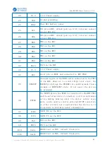
universal I /O pin.

4

IO4

universal I /O pin.

5

IRQ

The interrupt request output from the DWM1000 to the
host processor and is connected to the MCU PB0. by
default, the IRQ is a high-level efficient output, but
can be configured as low-level valid if required. to
run correctly in SLEEP and DEEPSLEEP mode, it should
be configured to run efficiently at high levels. this
pin will float in hibernation and DEEPSLEEP states and
may cause a pseudo interrupt unless it is pulled low.
This pin can be reconfigured as a generic I /O line
GPIO8. when no IRQ function is used

6

CLK

SPI clock and connected to MCU PA5

7

MISO

SPI data output and connected to MCU PA6

8

MOSI

SPI data input and connected to MCU PA7

9

CSN

SPI chip select and connect with MCU PA4. this is a low
level effective enable input. SPICSn jumps from high
to low indicate the beginning of a new SPI transaction.
SPICSn can also be used as a wake-up signal to get DW1000
out of sleep or sleep state.

10

PA3

PA3 on the MCU

11

PB1

PB1 on the MCU

12

PB10

PB10 on the MCU

13

PB11

PB11 on the MCU

14

LED1

PA2, connection LED1 on the MCU

15

LED2

PA1, connection LED2 on the MCU

16

BTN

PA0, connection BTN keys on the MCU

17

RESET

Reset pin on MCU, connect reset button

18

GND

Ground

19

GND

Ground

20

V3.3

3.3 V Power supply

21

V5

5V power supply

Содержание NodeMCU-BU01

Страница 1: ...NodeMCU BU01Specification V 1 0 Copyrigh t Shenzhen Ai Thinker Technology Co Ltd All Rights Reserved 2020 1 NodeMCU BU01 SPECIFICATION Version V1 0 Copyright 2020...

Страница 2: ...obtained from the testing performed by Anxinke Labs Actual results may vary slightly The Wi Fi Alliance member logo is owned by the Wi Fi Alliance All trademark names trademarks and registered tradema...

Страница 3: ...V 1 0 Copyrigh t Shenzhen Ai Thinker Technology Co Ltd All Rights Reserved 2020 3 Documentation revision revocation resume Version Date Development revision Developme nt Approval V1 0 2020 05 20 Init...

Страница 4: ...hnology Co Ltd All Rights Reserved 2020 4 Content 1 Product Overview 5 2 Electrical parameters 7 3 Appearance dimensions 8 4 Definition of pins 9 5 Schematic diagrams 12 6 Design guidance 12 7 ROLLING...

Страница 5: ...ransceiver module based on Decawave DW1000 design BU01 integrated the antenna RF circuit power management and clock circuits BU01 can be used in bidirectional ranging or TDOA positioning systems Posit...

Страница 6: ...Main parameters Table 1 Key parameter descriptions Model Name NodeMCU BU01 Dimensions 35 55 5 0 2 W H mm Package DIP 40 Antenna PCB antenna Frequency range 3 5GHz to 6 5GHz Interface The all IO of PWM...

Страница 7: ...parameters Electrical characteristics Absolute maximum rating Any more than the following absolute maximum ratings can cause chip damage Name of name Minimum value Typical values Maximum value Units M...

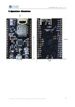
Страница 8: ...NodeMCU BU01Specification V 1 0 C opyright Shenzhen Ai Thinker Technology Co Ltd All Rights Reserved 2020 8 3 Appearance dimensions...

Страница 9: ...able Pin No Item Functional Description 1 IO7 default value is used as SYNC input this pin can be reconfigured as a universal I O pin GPIO7 under software control 2 IO6 universal I O pin when powered...

Страница 10: ...econfigured as a generic I O line GPIO8 when no IRQ function is used 6 CLK SPI clock and connected to MCU PA5 7 MISO SPI data output and connected to MCU PA6 8 MOSI SPI data input and connected to MCU...

Страница 11: ...12 35 WAKEUP the wake up pin on the BU01 and is connected to the PB13 of the MCU when set to a valid high level state the WAKEUP pin brings the DW1000 into working mode from a dormant or DEEPSLEEP sta...

Страница 12: ...oot on MCU control MCU start mode RESET keys RESET Reset button BTN PA0 keys BTN PA0 Press button to pull up PA0 pin BOOT pin controls start up mode BOOT0 BOOT1 MODE 0 x FLASH 1 1 SRAM 1 0 ISP 5 Schem...

Страница 13: ...3 V Power supply 1 recommend 3 3 V voltage peak over 500mA current 2 recommend the use of LDO power supply if used DC DC the recommended ripple is controlled within 30mV 3 DC DC power supply circuit...

Страница 14: ...NodeMCU BU01Specification V 1 0 C opyright Shenzhen Ai Thinker Technology Co Ltd All Rights Reserved 2020 14 7 ROLLING OF Reflow soldering...

Страница 15: ...9 Contact us Official website https www ai thinker com Development DOCS https docs ai thinker com Official Forum http bbs ai thinker com Sample purchase https anxinke taobao com Business cooperation...

Отзывы: