


PCIE-1816_1816H User Manual
16
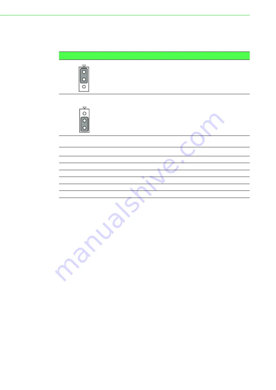
3.2.3
Jumper Settings to Set Ports as Software-configurable or
Output ports
Table 3.3: Function Description
Set DIO channel as software-configurable input or output (default)
Set DIO channel as output
Jumper number
Relative channels
JP1600
DIO 0~3
JP1601
DIO 4~7
JP1700
DIO 8~11
JP1701
DIO 12~15
JP1800
DIO 16~19
JP1801
DIO 20~23
Содержание PCIE-1816
Страница 1: ...User Manual PCIE 1816 1816H 16 bit Multi function Card with PCI Express Bus ...
Страница 4: ...PCIE 1816_1816H User Manual iv ...
Страница 10: ...PCIE 1816_1816H User Manual 4 Figure 1 1 Installation Flow Chart ...
Страница 36: ...PCIE 1816_1816H User Manual 30 ...
Страница 37: ...Appendix A A Specifications ...
Страница 38: ...PCIE 1816_1816H User Manual 32 A 1 Function Block ...
Страница 42: ...PCIE 1816_1816H User Manual 36 ...
Страница 43: ...Appendix B B Operation Theory ...
Страница 61: ...55 PCIE 1816_1816H User Manual Appendix B Operation Theory ...