background image

SERIES IP330 INDUSTRIAL I/O PACK                                  16-BIT HIGH DENSITY ANALOG INPUT MODULE 
___________________________________________________________________________________________


- 5 - 

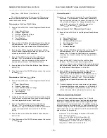
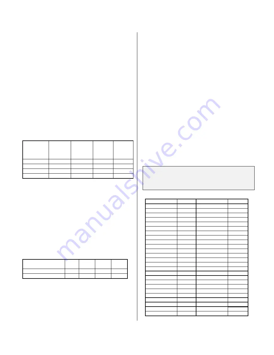
Default Hardware Jumper Configuration 


When the board is shipped from the factory, it is configured as 

follows: 


Analog input range is configured for a bipolar input with a 10 
volt span (i.e. an ADC input range of -5 to +5 Volts). 


In12 and -12 Volt power supplies are used (sourced 
from P1 connector). 


The default programmable software control register bits at 
power-up are described in section 3.  The control registers 
must be programmed to the desired gain, mode, and channel 
configuration before starting ADC analog input acquisition. 


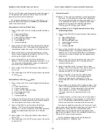
Analog Input Range Hardware Jumper Configuration 


The ADC input range is programmed via hardware DIP switch.  

The DIP switch controls the input voltage span and the selection of 
unipolar or bipolar input ranges.  The configuration of the DIP 
switch for the different ranges is shown in the following table.  A 
switch selected as "ON" would be positioned to the side of the DIP 
labeled “ON”.  The DIP switch location is shown in Drawing 4501-
590. 
 

Table 2.1:Analog Input Range Selections/DIP Switch Settings 

Desired 

ADC Input 

Range* 

(VDC) 

Required 

Input Span 

(Volts) 

Required 

Input 

Type 

Switch 

Settings 

ON 

Switch 

Settings 

OFF 

-5 to +5 

10 

Bipolar 

1,3,4,9 

2,5,6,7,8 

-10 to +10** 

20 

Bipolar 

2,5,6,9 

1,3,4,7,8 

0 to +5 

Unipolar 

1,3,5,8 

2,4,6,7,9 

0 to +10** 

10 

Unipolar 

1,3,4,7 

2,5,6,8,9 

*  Assuming a gain of 1. 
** These ranges can only be achieved with 

±

15V external power 

supplies.  The input ranges will be clipped if 

±

12V supplies are 

used, typically to 

±

8.5 V maximum inputs. 

 
Power Supply Hardware Jumper Configuration 


The selection of internal or external analog power supplies is 

accomplished via hardware jumpers J1 and J2.  J1 (J2) controls 
the selection of either the in12 (-12) Volt supply sourced 
from P1 connector, or the ex15 (-15) Volt supply sourced 
from the P2 connector.  The configuration of the jumpers for the 
different supplies is shown in Table 2.2.  "IN" means that the pins 
are shorted together with a shorting clip.  "OUT" means that the 
clip has been removed.  The jumper locations are shown in 
Drawing 4501-590. 
 

Table 2.2: Power Supply Selections (Pins of J1 and J2) 

Power Supply 

Selection* 

J1 

(1&2) 

J1 

(2&3) 

J2 

(1&2) 

J2 

(2&3) 

±

12 Volt (Internal, P1) 

OUT 

IN 

OUT 

IN 

±

15 Volt (External, P2) 

IN 

OUT 

IN 

OUT 

*  Internal and external supplies should not be mixed (e.g. do not 

use +12 Volts with -15 Volts). 


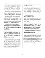
Software Configuration 


Software configurable control registers are provided for control 

of external trigger mode, data output format, acquisition mode, 
timer control, interrupt mode, convert channel(s) selection, and 
channel gain selection.  No hardware jumpers are required for 

control of these functions.  These control registers must also be 
configured as desired before starting ADC analog input 
acquisition.  Refer to section 3 for programming details.  

 
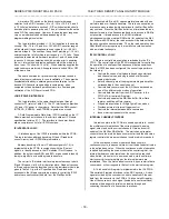
CONNECTORS 


IP Field I/O Connector (P2) 

P2 provides the field I/O interface connections for mating IP 

modules to the carrier board.  P2 is a 50-pin female receptacle 
header (AMP 173279-3 or equivalent) which mates to the male 
connector of the carrier board (AMP 173280-3 or equivalent).  This 
provides excellent connection integrity and utilizes gold-plating in 
the mating area.  Threaded metric M2 screws and spacers are 
supplied with the module to provide additional stability for harsh 
environments (see Mechanical Assembly Drawing 4501-434).  The 
field and logic side connectors are keyed to avoid incorrect 
assembly.   

 
P2 pin assignments are unique to each IP model (see Table 

2.3) and normally correspond to the pin numbers of the field I/O 
interface connector on the carrier board (you should verify this for 
your carrier board).  When reading Table 2.3 note that channel 
designations are abbreviated to save space.  For example, single 
ended channel 0 is abbreviated as “S00”; the +input for differential 
channel 0 is abbreviated as “D00+”.  Both of these labels are 
attached to pin 1, but only one is active for a particular installation 
(i.e. if your inputs are applied differentially, which is recommended 
for the lowest noise and best accuracy, follow the differential 
channel labeling for each channel’s + and - input leads). 

 
IMPORTANT:  All unused analog input pins should be tied to 

analog gorund.  Floating unused inputs can drift outside the input 
range causing temporary saturation of the input analog circuits.  
Recovery from saturation is slow and affects the reading of the 
desired channels. 

 
Table 2.3:  IP330 Field I/O Pin Connections (P2) 

Pin 

Description Number Pin 

Description  Number 

S00,D00+ 1  S24,D08- 26 

S16,D00- 2 COMMON 27 

COMMON 3 S09,D09+ 28 

S01,D01+ 4  S25,D09- 29 

S17,D01- 5 COMMON 30 

COMMON 6 S10,D10+ 31 

S02,D02+ 7  S26,D10- 32 

S18,D02- 8 COMMON 33 

COMMON 9 S11,D11+ 34 

S03,D03+ 10 S27,D11-  35 

S19,D03- 11 COMMON 36 

COMMON 12 S12,D12+  37 

S04,D04+ 13 S28,D12-  38 

S20,D04- 14 COMMON 39 

COMMON 15 S13,D13+  40 

S05,D05+ 16 S29,D13-  41 

S21,D05- 17  SENSE  42 

COMMON 18 S14,D14+  43 

S06,D06+ 19 S30,D14-  44 

S22,D06- 20 +15 

VOLTS 45 

COMMON 21 S15,D15+  46 

S07,D07+ 22 S31,D15-  47 

S23,D07- 23 -15 

VOLTS 48 

COMMON 24 

EXT 

TRIGGER* 

49 

S08,D08+ 25  SHIELD  50 

Indicates that the signal is active low. 

Содержание IP330 Series

Страница 1: ...ut Module USER S MANUAL ACROMAG INCORPORATED 30765 South Wixom Road P O BOX 437 Wixom MI 48393 7037 U S A Tel 248 624 1541 Fax 248 624 9234 Copyright 1995 Acromag Inc Printed in the USA Data and speci...

Страница 2: ...NCE 19 PRELIMINARY SERVICE PROCEDURE 19 6 0 SPECIFICATIONS 20 GENERAL SPECIFICATIONS 20 ANALOG INPUT 20 INDUSTRIAL I O PACK COMPLIANCE 21 APPENDIX 21 CABLE MODEL 5025 551 21 Recommended APC8600 Shiele...

Страница 3: ...le ended channels Precision On Board Calibration Voltages Calibration autozero and autospan precision voltages are available to permit host computer correction of conversion errors Trimmed calibration...

Страница 4: ...Library diskette Model IPSW LIB M03 MSDOS format to simplify communication with the board Example software functions are provided for both VMEbus and ISA bus PC AT applications All functions are writ...

Страница 5: ...iguration Software configurable control registers are provided for control of external trigger mode data output format acquisition mode timer control interrupt mode convert channel s selection and cha...

Страница 6: ...l has been driven low it should remain low for a minimum of 500n seconds As an output an active low TTL signal can be driven to additional IP330s thus providing a means to synchronize the conversions...

Страница 7: ...elect Ch 07 27 28 Gain Select Ch 08 Gain Select Ch 09 29 2A Gain Select Ch 10 Gain Select Ch 11 2B 2C Gain Select Ch 12 Gain Select Ch 13 2D 2E Gain Select Ch 14 Gain Select Ch 15 2F 30 Gain Select Ch...

Страница 8: ...10 Uniform Single 011 Burst Continuous 100 Burst Single 101 Convert on External Trigger Only 110 Not Used 111 Not Used See the Modes of Operation section for a description of each of these scan modes...

Страница 9: ...z clock signal The output of this clock is input to the second counter the Conversion Timer and the output is used to generate periodic trigger pulses The time period between trigger pulses is describ...

Страница 10: ...y 0CH Data Bit 15 14 13 12 11 10 09 08 SE or Diff Ch 15 14 13 12 11 10 09 08 Missed Data Register Read Only 0FH Data Bit 07 06 05 04 03 02 01 00 SE Channel 23 22 21 20 19 18 17 16 Diff Channel 07 06 0...

Страница 11: ...niform continuous uniform single burst continuous burst single and convert on external trigger only In all modes a single channel or a sequence of channels may be converted The following sections desc...

Страница 12: ...Box functions as a dual level data buffer The first half of the Mail Box is used to store all selected channel data for the initial pass through the channels defined by the Start and End Value regist...

Страница 13: ...external trigger pulse no interrupt will be issued since data is not written to the Mail Box buffer If interrupt upon completion of a group of channels is selected an interrupt will be issued 8 secon...

Страница 14: ...5 2 0 to 5 0 6125 CAL3 2 4500 CAL1 Input Range Volts PGA Gain ADC Range Volts Rec Low Calib Voltage VoltCALLO Volts Rec High Calib Voltage VoltCALHI Volts 0 to 1 25 4 0 to 5 0 6125 CAL3 1 2250 CAL2 0...

Страница 15: ...are known It is now possible to correct input channel data from any input channel using the same input range i e 10 to 10 volts with a PGA gain 1 Repeat the above steps periodically to re measure the...

Страница 16: ...CountCALHI Calculate Equation 2 Calculate m actual_slope from equation 2 since all parameters are known It is now possible to correct input channel data from any input channel using the same input ra...

Страница 17: ...he host uses the vector to form a pointer to an interrupt service routine for the interrupt handler to begin execution 7 Example of Generic Interrupt Handler Actions a Disable the interrupting IP by w...

Страница 18: ...from the Mail Box buffer Access to both ID and I O spaces are implemented with one wait state read or write data transfers There is one exception on a rare occasions read and write operations to the M...

Страница 19: ...r is clocked by the 8MHz board clock The output of the Timer Prescaler counter is then used to clock the second counter Conversion Timer In this way the two counters are cascaded to provide variable t...

Страница 20: ...ware limitations For example if an input may reach zero volts or less a bipolar input range should be selected 4 These ranges can only be achieved with 15 Volt external power supplies The input ranges...

Страница 21: ...E Specification This module meets or exceeds all written Industrial I O Pack specifications per revision 0 7 1 Electrical Mechanical Interface Single Size IP Module IP Data Transfer Cycle Types Suppor...

Страница 22: ...he field I O signals to the P2 connector on each of the Industrial I O Pack modules Field signals are accessed via screw terminal strips Each Industrial I O Pack IP has its own unique P2 pin assignmen...

Страница 23: ...SERIES IP330 INDUSTRIAL I O PACK 16 BIT HIGH DENSITY ANALOG INPUT MODULE ___________________________________________________________________________________________ 23...

Страница 24: ...SERIES IP330 INDUSTRIAL I O PACK 16 BIT HIGH DENSITY ANALOG INPUT MODULE ___________________________________________________________________________________________ 24...

Страница 25: ...SERIES IP330 INDUSTRIAL I O PACK 16 BIT HIGH DENSITY ANALOG INPUT MODULE ___________________________________________________________________________________________ 25...

Страница 26: ...SERIES IP330 INDUSTRIAL I O PACK 16 BIT HIGH DENSITY ANALOG INPUT MODULE ___________________________________________________________________________________________ 26...

Страница 27: ...SERIES IP330 INDUSTRIAL I O PACK 16 BIT HIGH DENSITY ANALOG INPUT MODULE ___________________________________________________________________________________________ 27...

Страница 28: ...SERIES IP330 INDUSTRIAL I O PACK 16 BIT HIGH DENSITY ANALOG INPUT MODULE ___________________________________________________________________________________________ 28...

Отзывы: