background image


INTRODUCTION


CHAPTER


1


This chapter gives you the information for PC 1060. Itso 
outlines the System specifications. 


Section includes: 


z

 About This Manual 


z

 Case Illustration 


z

 System Specifications 


z

 Safety precautions 


for a Quick Start.


page 2-1


Page:1-1


Содержание PC 1060

Страница 1: ...USER MANUAL PC 1060 VIA Eden Low Power 10 4 PanelPC System...

Страница 2: ...ny notice This manual is copyrighted November 2004 You may not reproduce or transmit in any form or by any means electronic or mechanical including photocopying and recording ACKNOWLEDGEMENTS All trad...

Страница 3: ...case the user will be required to correct the interference at his own expense You are cautioned that any change or modifications to the equipment not expressly approve by the party responsible for co...

Страница 4: ...tage Selection 2 13 2 10 LVDS Voltage Selection 2 14 2 11 Power Connector 2 15 2 12 Floppy Disk Drive Connector 2 16 2 13 Hard Disk Drive Connector 2 17 2 14 Printer Connector 2 18 2 15 LAN Connector...

Страница 5: ...GA Driver Utility 3 3 3 4 Flash BIOS Update 3 4 3 5 LAN Driver Utility 3 6 3 6 Sound Driver Utility 3 7 3 7 USB2 0 Chipset Software Installation Utility 3 8 3 8 Touch Screen Driver Utility Optional 3...

Страница 6: ...m for Whole System Unit A 2 Exploded Diagram for Removing Hook Holder A 3 Exploded Diagram for Removing Back Cover A 4 Exploded Diagram for Removing LCD Assembly A 5 Exploded Diagram for Front Panel A...

Страница 7: ...s chapter gives you the information for PC 1060 Itso outlines the System specifications Section includes z About This Manual z Case Illustration z System Specifications z Safety precautions for a Quic...

Страница 8: ...e final page of this chapter indicates some safety reminders on how to take care of your system Chapter 2 System Configuration This chapter outlines the components locations and their functions In the...

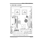
Страница 9: ...Chapter 1 Introduction 1 2 CASE ILLUSTRATION PC 1060 USER S MANUAL Page 1 3...

Страница 10: ...Chapter 1 Introduction Page 1 4 PC 1060 USER S MANUAL...

Страница 11: ...board z CACHE Built in CPU 128 256KB Cache z REAL TIME CLOCK CR2023 battery backed CMOS RAM Hardware implementation to indicate century rollover z BIOS Phoenix Award Flash BIOS for plug play function...

Страница 12: ...lectable for NMI or Reset function Time out timing select 0 8 16 24 32 40 48 56 64 72 80 88 96 104 112 120 sec 25 z IDE INTERFACE 1 EIDE UDMA 33 onboard 1 Compact Flash Type II onboard z FLOPPY DISK D...

Страница 13: ...anel 2 internal USB ports on board Internal USB ports use 2 0 pitch box header for connection All USB ports support USB 1 1 standard z SOUND VT1612A AC 97 Codec MIC in SPK out jacks on rear panel Anot...

Страница 14: ...upplier s LCD specification z CONTRAST RATIO According to the supplier s LCD specification z POWER CONSUMPTION According to the supplier s LCD specification z VIEWING ANGLE According to the supplier s...

Страница 15: ...NERAL INFORMATION z POWER SUPPLY DC 15V 24V input ATX 80W 10 Pin output Or AC 100V 240V 50 60Hz input Protech ATX 100W Built in z DRIVE BAYS Optional 1x Slim HDD 1x Compact Flash Type II Slot IDE On B...

Страница 16: ...cold place or vice versa because condensation may come from inside of the system f Place PPC against strong vibrations which may cause hard disk failure g Do not place the system too close to any radi...

Страница 17: ...ul information that describes the jumper connecto settings and component locations Section includes z Jumper Connector Quick Reference Table z Component Locations z Configuration and Jumper settings z...

Страница 18: ...nector LINE1 MIC1 SPK1 Onboard Audio Selection JP11 Reset Connector JP17 HDD LED Connector HDLED1 Power Button CN56 External Buzzer Connector JP14 1 2 External SMI Connector JP14 7 8 CMOS Function Sel...

Страница 19: ...Chapter 2 Hardware Configuration 2 2 COMPONENT LOCATIONS PC 1060 Connector Jumper and Component locations PC 1060 USER S MANUAL Page 2 3...

Страница 20: ...pins The jumper can be combined into sets that called jumper blocks When the jumpers are all in the block you have to put them together to set up the hardware configuration The figure below shows how...

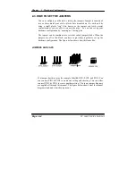
Страница 21: ...Chapter 2 Hardware Configuration JUMPER DIAGRAMS JUMPER SETTINGS PC 1060 USER S MANUAL Page 2 5...

Страница 22: ...r assignments are as follows PIN ASSIGNMENT 1 COM1 DCD 2 COM1 RXD 3 COM1 TXD 4 COM1 DTR 5 GND 6 COM1 DSR 7 COM1 RTS 8 COM1 CTS 9 COM1 RI 5V 12V selectable COM1 COM2 COM2 Connector The COM2 Connector a...

Страница 23: ...3 CTS 9 COM3 RI 5V 12V selectable 10 NC COM4 COM4 Connector The pin assignments are as follows PIN ASSIGNMENT 1 COM4 DCD 2 COM4 RX 3 COM4 TX 4 COM4 DTR 5 GND 6 COM4 DSR 7 COM4 RTS 8 COM4 CTS 9 COM4 RI...

Страница 24: ...I VOLTAGE SELECTION JP19 COM1 COM2 COM3 and COM4 RI Voltage Selection The selections are as follows SELECTION JUMPER SETTING Pin Closed RI 1 2 JUMPER ILLUSTRATION COM1 COM2 5V 11 13 12V 9 11 RI 3 4 5V...

Страница 25: ...Chapter 2 Hardware Configuration RI 5 6 COM3 COM4 5V 15 17 12V 17 19 RI 7 8 5V 16 18 12V 18 20 PC 1060 USER S MANUAL Page 2 9...

Страница 26: ...ectable for RS 232 422 485 function The jumper settings are as follows COM 2 FUNCTION JUMPER SETTING pin closed JUMPER ILLUSTRATION RS 232 Open RS 422 1 2 5 6 7 8 9 10 11 12 13 14 15 16 17 18 19 20 RS...

Страница 27: ...2 7 VGA CONNECTOR VGA VGA Connector The pin assignments are as follows PIN ASSIGNMENT 1 RED 2 GREEN 3 BLUE 4 NC 5 GND 6 GND 7 GND 8 GND 9 VCC 10 GND 11 NC 12 PULL HI 13 HSYNC 14 VSYNC 15 PULL HI 16 NC...

Страница 28: ...Y2P 14 GND 4 NC 15 Y0P 5 Y2M 16 GND 6 NC 17 Y0M 7 GND 18 LVDSVCC 8 GND 19 GND 9 Y1P 20 LVDSVCC 10 YCP 11 Y1M LVDS2 LVDS Connector The pin assignments are as follows PIN ASSIGNMENT PIN ASSIGNMENT 1 GN...

Страница 29: ...9 BRIGHTNESS VOLTAGE SELECTION JP9 Brightness Voltage Selection The selections are as follows SELECTION JUMPER SETTING Pin Closed 5V 2 3 2 5V 1 2 JUMPER ILLUSTRATION Manufacturing Default is set as 5...

Страница 30: ...2 10 LVDS VOLTAGE SELECTION JP12 LCD Voltage Selection The selections are as follows SELECTION JUMPER SETTING Pin Closed 12V 1 2 3 3V 3 4 5V 5 6 JUMPER ILLUSTRATION Manufacturing Default is set as 3 3...

Страница 31: ...rdware Configuration 2 11 POWER CONNECTOR CN1 Power Connector The pin assignments are as follows PIN ASSIGNMENT 1 VCC 2 VCC 3 GND 4 GND 5 VCC12 6 5VSB 7 VCC 8 GND 9 PS_ON 10 VCC12J PC 1060 USER S MANU...

Страница 32: ...ector The pin assignments are as follows PIN ASSIGNMENT PIN ASSIGNMENT 2 INDEX 1 VCC 4 DRVA 3 VCC 6 DSKCHG 5 VCC 8 NC 7 NC 10 MOTEA 9 NC 12 FDIR 11 NC 14 STEP 13 DENSEL 16 WDATA 15 NC 18 WGATE 17 GND...

Страница 33: ...PDD7 4 PDD8 5 PDD6 6 PDD9 7 PDD5 8 PDD10 9 PDD4 10 PDD11 11 PDD3 12 PDD12 13 PDD2 14 PDD13 15 PDD1 16 PDD14 17 PDD0 18 PDD15 19 GND 20 NC 21 DDREQA 22 GND 23 DIOWAJ 24 GND 25 DIORAJ 26 GND 27 HDRDYA 2...

Страница 34: ...connect both DB25 connector and parallel port The pin assignments are as follows LPT1 PIN ASSIGNMENT PIN ASSIGNMENT 1 STROBE 14 AUTOF 2 PPD0 15 ERROR 3 PPD1 16 INIT 4 PPD2 17 SLCTIN 5 PPD3 18 GND 6 PP...

Страница 35: ...pin assignment is as follows PIN ASSIGNMENT 1 MDI_0P 2 MDI_0N 3 MDI_1P 4 MDI_2P 5 MDI_2N 6 MDI_1N 7 MDI_3P 8 MDI_3N 2 16 LAN LED CONNECTOR LANLED1 LAN LED Connector The pin assignment is as follows P...

Страница 36: ...ssignments are as follows PIN ASSIGNMENT 1 KB DATA 6 5 2 NC 4 3 3 GND 1 2 4 KBMFVCC 5 KB CLK 6 NC KB1 2 18 PS 2 MOUSE CONNECTOR MS1 PS 2 Mouse Connector The pin assignments are as follows PIN ASSIGNME...

Страница 37: ...INE1 LINE1 Line In Connector The pin assignment is as follows PIN ASSIGNMENT 1 GND 2 LINE_L 3 LINE_R MIC1 Microphone Connector The pin assignment is as follows PIN ASSIGNMENT 1 GND 2 MIC IN 3 MIC VDD...

Страница 38: ...R SETTING pin closed JUMPER ILLUSTRATION On 1 2 Off open Manufacturing Default On 2 21 RESET CONNECTOR JP17 Reset Connector The pin assignment is as follows PIN ASSIGNMENT 1 GND 2 RSTSW 2 22 HDD LED C...

Страница 39: ...NMENT 1 PW BN 2 GND 2 24 EXTERNAL BUZZER CONNECTOR JP14 1 2 External Buzzer Connector The pin assignments are as follows PIN ASSIGNMENT 1 E_BUZ_PWR 2 E_BUZ 2 25 EXTERNAL SMI CONNECTOR JP14 7 8 Externa...

Страница 40: ...ION JUMPER SETTING pin closed JUMPER ILLUSTRATION NORMAL 1 2 CLEAR CMOS 2 3 Manufacturing Default Normal To clear CMOS data user must power off the computer and set the jumper to Clear CMOS as illustr...

Страница 41: ...ows PIN ASSIGNMENT 1 USBV0 2 USB_DDT0 3 USB_DDT0 4 GND USB2 Universal Serial Bus Connector The pin assignments are as follows PIN ASSIGNMENT 1 USBV1 2 USB_DDT1 3 USB_DDT1 4 GND USB3 Universal Serial B...

Страница 42: ...ws FUNCTION JUMPER SETTING Reset 1 2 NMI 3 4 JUMPER ILLUSTRATION Manufacturing Default is set as Reset User may select to use the Reset or NMI watchdog NMI also known as Non Maskable Interrupt is used...

Страница 43: ...B 2 GND 3 WOL1 2 30 POWER LED CONNECTOR PWLED1 Power LED Connector The pin assignments are as follows PIN ASSIGNMENT 1 PWLED_PWR 2 GND 2 31 MEMORY INSTALLATION This system is enhanced with 1 DDR DRAM...

Страница 44: ...T ATX POWER SELECTION JP14 3 6 AT ATX Power Selection The selections are as follows FUNCTION JUMPER SETTING JP14 3 6 JP18 JUMPER ILLUSTRATION AT 3 4 5 6 Open ATX open 1 2 Manufacturing Default is set...

Страница 45: ...ows FUNCTION JUMPER SETTING Master 1 2 Slave open JUMPER ILLUSTRATION Manufacturing Default is set as Master 2 34 IRQ12 RELEASE SELECTION JP6 IRQ12 Release Selection The selections are as follows SELE...

Страница 46: ...lections are as follows FUNCTION JUMPER SETTING pin closed 800 x 600 10 4 1 2 1024 x 768 15 3 4 Manufacturing Default 800 x 600 2 36 INVERTER CONNECTOR INV1 Inverter Connector The pin assignments are...

Страница 47: ...N ASSIGNMENT 1 VCC 2 5VSB 3 VCC 4 5VSB 5 VCC 6 5VSB 7 VCC 8 VCC 9 VCC 10 VCC 11 VCC 12 VCC 13 GND 14 GND 15 GND 16 GND 17 GND 18 GND 19 PS ON 20 GND 21 NC 22 GND 23 NC 24 GND 25 VCC12J 26 VCC12 27 VCC...

Страница 48: ...D04 28 D121 4 D05 29 D131 5 D06 30 D141 6 D07 31 D151 7 CS0 32 CS11 8 A102 33 VS1 9 ATASEL 34 IORD 10 A092 35 IOWR 11 A082 36 WE3 12 3 3V 37 INTRQ 13 VCC 38 VCC 14 A062 39 CSEL 15 A052 40 VS2 16 A042...

Страница 49: ...CC12 C9 LA17 D9 DACK0 A10 IOCHRDY B10 GND C10 MEMR D10 DRQ0 A11 AEN B11 SMEMW C11 MEMW D11 DACK5 A12 A19 B12 SMEMR C12 D8 D12 DRQ5 A13 A18 B13 IOW C13 D9 D13 DACK6 A14 A17 B14 IOR C14 D10 D14 DRQ6 A15...

Страница 50: ...1 LOCK D11 GND A12 3 3V B12 TRDY C12 GND D12 DEVSEL A13 FRAME B13 GND C13 IRDY D13 3 3V A14 GND B14 AD16 C14 3 3V D14 C BE2 A15 AD18 B15 3 3V C15 AD17 D15 GND A16 AD21 B16 AD20 C16 GND D16 AD19 A17 3...

Страница 51: ...NNECTOR FAN1 CPU Fan Connector The pin assignments are as follows PIN ASSIGNMENT 1 GND 2 12V 3 CPUFAN1 2 42 SYSTEM FAN CONNECTOR FAN2 System FAN Connector The pin assignments are as follows PIN ASSIGN...

Страница 52: ...ash BIOS update It also describes how to install the watchdog timer configuration Section includes z Introduction z VIA 4 IN1 Service Pack Driver Utility z VGA Driver Utility z Flash BIOS Update z LAN...

Страница 53: ...D USB2 0 Drv USB 2 0 Software Installation Utility For Win 98SE 2000 ME XP D Touch Screen Drv For Liyi Touch screen driver D USB CF Card Drv For USB CF Card Driver Installation 3 2 VIA 4IN1 SERVICE P...

Страница 54: ...e embedded with our PC 1060 can support a wide range of display mode such as SVGA STN TFT etc You can display CRT and LCD Panel simultaneously on this board but make sure that the modes for CRT and LC...

Страница 55: ...SPLAY icon to start the DISPLAY PROPERTIES window then choose the SETTING tab then DISPLAY TYPE 3 In the CHANGE DISPLAY TYPE window click on the CHANGE button in the ADAPTER TYPE this will bring up th...

Страница 56: ...you choose N the following table will appear on screen FLASH MEMORY WRITER V7 XX C Award Software 2001 All Rights Reserved Flash Type MX29F004T File Name to Program s55xxxxx bin Error Message Are You...

Страница 57: ...pdate Write Fail F1 Reset F10 Exit Please reset or power off the system then the Flash BIOS is fully implemented 3 5 LAN DRIVER UTILITY 3 5 1 Introduction The PC 1060 Panel PC is enhanced with LAN fun...

Страница 58: ...Network icon 3 In the Network Settings dialog box choose the Add adapter button The Add Network Adapter dialog box appears 4 In the list of network cards select Other requires disk from manufacturer...

Страница 59: ...ATION UTILITY 3 7 1 Installation of Utility for Windows 98SE 2000 XP Intel USB 2 0 Enhanced Host Controller driver can only be used on Windows 98SE Windows 2000 and Windows XP on Intel Desktop boards...

Страница 60: ...43H When you want to enable the watchdog timer please write I O port 443H and then the system will either reset itself or perform the NMI function Likewise when you want to disable the function write...

Страница 61: ...TDX AX The Watchdog Timer control table is as follows Level Value Time sec Level Value Time sec 1 F 0 9 7 64 2 E 8 10 6 72 3 D 16 11 5 80 4 C 24 12 4 88 5 B 32 13 3 96 6 A 40 14 2 104 7 9 48 15 1 112...

Страница 62: ...tup z The Standard CMOS Features z The Advanced BIOS Features z The Advanced Chipset Features z Integrated Peripherals z Power Management Setup z PNP PCI Configurations z PC Health Status z Frequency...

Страница 63: ...spreadsheets and games rely on an operating system such as DOS or OS 2 to manage such things as keyboard monitor disk drives and memory The operating system relies on the BIOS Basic Input and Output...

Страница 64: ...the screen Phoenix AwardBIOS CMOS Setup Utility Standard CMOS Features Advanced BIOS Features Advanced Chipset Features Integrated Peripherals Power Management Setup PnP PCI Configurations PC Health...

Страница 65: ...All But Keyboard 640K 113664K 114688K Item Help Menu Level Change the day month year and century npom Move Enter Select PU PD Value F10 Save ESC Exit F1 General Help F5 Previous Values F6 Fail Safe D...

Страница 66: ...drive specifications x Type The BIOS contains a table of pre defined drive types Each defined drive type has a specified number of cylinders number of heads write precompensation factor landing zone a...

Страница 67: ...e to select the type in Setup Available Options are as follows EGA VGA Enhanced Graphics Adapter Video Graphics Array For EGA VGA SEGA SVGA or PGA monitor adapters CGA 40 Color Graphics Adapter power...

Страница 68: ...733 5 300 732 17 30 21 733 7 300 732 17 42 22 733 5 300 733 17 30 23 306 4 0000 336 17 10 24 977 5 65535 976 17 40 25 1024 9 65535 1023 17 76 26 1224 7 65535 1223 17 71 27 1224 11 65535 1223 17 111 28...

Страница 69: ...ect for DRAM 64MB Video BIOS Shadow C8000 CBFFF Shadow CC000 CFFFF Shadow D0000 D3FFF Shadow D4000 D7FFF Shadow D8000 DBFFF Shadow DC000 DFFFF Shadow Small Logo EPA Show Enabled Enabled Enabled Enable...

Страница 70: ...ains ECC SRAMs QUICK POWER ON SELF TEST This item allows you to speed up Power On Self Test POST after power up the computer When enabled the BIOS will shorten or skip some check items during POST FIR...

Страница 71: ...stroke when you hold the key down TYPEMATIC DELAY MSEC The item sets the delay time after the key is held down before it begins to repeat the keystroke SECURITY OPTION This category allows you to lim...

Страница 72: ...Concurrency System BIOS Cacheable Video RAM Cacheable Frame Buffer Size Panel Controlled By X Panel Resolution Boot Device Select OnChip USB USB Keyboard Support OnChip Sound CPU to PCI Write Buffer P...

Страница 73: ...e in this field depends on performance parameters of the installed memory chips DRAM Do not change the value from the factory setting unless you install new memory that has a different performance rat...

Страница 74: ...oard and you want to use it Even when so equipped if you add a higher performance controller you will need to disable this feature USB KEYBOARD SUPPORT Select Enabled if your system contains a Univers...

Страница 75: ...rt delay transactions cycles Select Enabled to support compliance with PCI specification version 2 1 PCI 2 ACCESS 1 RETRY When disabled PCI 2 will not be disconnected until access finishes default Whe...

Страница 76: ...lel Port Onboard Parallel Mode X ECP Mode Use DMA X Parallel Port EPP Type Onboard Parallel Port 3 Serial Port 3 Use IRQ Onboard Serial Port 4 Serial Port 4 Use IRQ IO Channel Check NMI Watch Dog Time...

Страница 77: ...ch device PRIMARY MASTER SLAVE UDMA SECONDARY MASTER SLAVE UDMA Ultra DMA 33 implementation is possible only if your IDE hard drive supports it and the operating environment includes a DMA driver Wind...

Страница 78: ...the onboard parallel printer port Select Normal Compatible or SPP unless you are certain your hardware and software both support one of the other available modes ECP MODE USE DMA Select a DMA channel...

Страница 79: ...Defaults F7 Optimized Defaults Power Management Setup Screen The Power Management Setup allows the user to configure the system to the most effectively save energy while operating in a manner consist...

Страница 80: ...es blanks to the video buffer DPMS Select this option if your monitor supports the Display Power Management Signalling DPMS standard of the Video Electronics Standards to select video power management...

Страница 81: ...you need the BIOS to configure non boot devices npom Move Enter Select PU PD Value F10 Save ESC Exit F1 General Help F5 Previous Values F6 Fail Safe Defaults F7 Optimized Defaults PNP PCI Configuratio...

Страница 82: ...lutely nothing unless you are using a Plug and Play operating system such as Windows 95 By choosing manual you are allowed to configure the IRQ Resources DMA Resources and Memory Resources The choices...

Страница 83: ...e ESC Exit F1 General Help F5 Previous Values F6 Fail Safe Defaults F7 Optimized Defaults PC Health Status Setup Screen The setup menu allows you to select whether to choose between monitoring or igno...

Страница 84: ...read Spectrum Disabled Menu Level npom Move Enter Select PU PD Value F10 Save ESC Exit F1 General Help F5 Previous Values F6 Fail Safe Defaults F7 Optimized Defaults Frequency Voltage Control Setup Sc...

Страница 85: ...ower up the system Please be aware that if select the wrong panel type it may cause the abnormal display of the LCD 4 12 LOAD OPTIMIZED DEFAULTS When you press Enter on this category you get a confirm...

Страница 86: ...ssword typed now will clear any previously entered password from CMOS memory You will be asked to confirm the password Type the password again and press the Enter key You may also press Esc to abort t...

Страница 87: ...ipherals Frequency Voltage Control Load Fail Safe Defaults Load Optimized Defaults Set Supervisor Password Power Management PnP PCI Configura PC Health Status Save to CMOS and EXIT Y N Y word etup Sav...

Страница 88: ...Phoenix AwardBIOS CMOS Setup Utility Standard CMOS Features Advanced BIOS Features Advanced Chipset Features Integrated Peripherals Frequency Voltage Control Load Fail Safe Defaults Load Optimized Def...

Страница 89: ...diagram of the system Section includes z Exploded Diagram for Whole System Unit z Exploded Diagram for Removing Hook Holder z Exploded Diagram for Removing Back Cover z Exploded Diagram for Removing...

Страница 90: ...Appendix A System Assembly EXPLODED DIAGRAM FOR WHOLE SYTEM UNIT Page A 2 PC 1060 USER MANUAL...

Страница 91: ...Appendix A System Assembly EXPLODED DIAGRAM FOR REMOVING HOOK HOLDER PC 1060 USER MANUAL Page A 3...

Страница 92: ...Appendix A System Assembly EXPLODED DIAGRAM FOR REMOVING BACK COVER Page A 4 PC 1060 USER MANUAL...

Страница 93: ...Appendix A System Assembly EXPLODED DIAGRAM FOR REMOVING LCD ASSEMBLY PC 1060 USER MANUAL Page A 5...

Страница 94: ...Appendix A System Assembly EXPLODED DIAGRAM FOR FRONT PANEL Page A 6 PC 1060 USER MANUAL...

Страница 95: ...TECHNICAL SUMMARY APPENDIX B This section introduce you the maps concisely Sections include z Block Diagram z Interrupt Map z RTC Standard RAM Bank z Timer DMA Channels Map z I O Memory Map Page B 1...

Страница 96: ...Appendix B Technical Summary BLOCK DIAGRAM Page B 2 PC 1060 USER MANUAL...

Страница 97: ...rd output buffer full 2 Cascade for IRQ 8 15 3 Serial port 2 4 Serial port 1 5 Available 6 Floppy Disk adapter 7 Parallel port 1 8 RTC clock 9 ACPI Compliant System 10 Serial port 3 11 Serial port 4 1...

Страница 98: ...nds 01h Second alarm 02h Minutes 03h Minutes alarm 04h Hours 05h Hours alarm 06h Day of week 07h Day of month 08h Month 09h Year 0Ah Status register A 0Bh Status register B 0Ch Status register C 0Dh S...

Страница 99: ...Timer Channel Assignment 0 System timer interrupt 1 DRAM Refresh request 2 Speaker tone generator DMA Channel Map DMA Channel Assignment 0 Available 1 Available 2 Floppy Disk adapter 3 Available 4 Cas...

Страница 100: ...ler Interrupt 3Ch 3Dh Interrupt Controller Interrupt Controller Interrupt 40h 42h Timer Counter Timer Counter PIT 8254 43h Reserved Timer Counter PIT 4E 4F LPC SIO LPC SIO Forwarder to LPC 50h 52h Tim...

Страница 101: ...wer Management Power Management B4h B5h Interrupt Controller Interrupt Controller Interrupt B8h B9h Interrupt Controller Interrupt Controller Interrupt BCh BDh Interrupt Controller Interrupt Controlle...

Страница 102: ...0h FF3F FFFFh FF60 0000h FF6F FFFFh FF20 0000h FF2F FFFFh FF50 0000h FF5F FFFFh FF10 0000h FF1F FFFFh FF40 0000h FF4F FFFFh FF00 0000h FF0F FFFFh FWH Bit 0 in FWH Decode Enable Register FWH Bit 1 in F...

Отзывы: