background image

1.3.2.6 Abnormal Signal Immunity

The monitor shall not be damaged by improper sync

timing , pulse duration , or absence of sync , or

abnormal input signal amplitude ( video and/ or sync

too large or too small) , or any other anomalous

behavior of a graphics card video generator when

changing modes , or when any combination of input

signals is removed or replaced . Additionally , under

these conditions , the monitor shall not cause

damage to the driving source

1.3.3 User Controls and Indicators

1.3.3.1Power On / Off Switch

The monitor shall have a power control switch

visible and accessible on the front of the monitor .

The switch shall be marked with icons per IEC 417 ,

# 5007 and # 5009.The switch shall interrupt the DC

supply to the monitor

1.3.3.2 Power Indicator LED

The monitor shall make use of an LED type

indicator located on the front of the monitor .

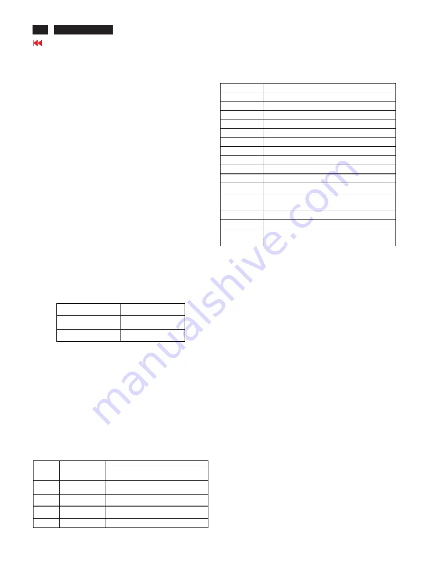
The LED color shall indicate the power states as

given in Table 1.

1.3.4 Monitor Modes and Timing Capability

1.3.4.1 Format and Timing

The monitor shall synchronize with any vertical

frequency from 55 to 76 Hz , and with any

horizontal frequency from 30 to 94KHz. If the input

frequency is out of the above – specified range,

the monitor shall display a warning screen

indicating that the input frequency is out of range.

Under no circumstances shall any combination of

input signals cause any damage to the monitor .

1.3.4.2 Factory Assigned Display Modes

There are 24 factory pre-set frequency video

modes. These modes have a factory pre-set for all

characteristics affecting front-of-screen

performance. When the system is powered-

on,previously stored screen parameters for a pre-

defined mode will be recalled if the operating

mode is one of those stored in memory. If the

operating mode is not one of those stored in

memory, the monitor CPU will select the PRESET

timing for a mode that is the next lowest in

horizontal scanning frequency to the mode being

currently used. The screen parameters may be

adjusted by the use of the front bezel controls and

then may be saved as a user defined mode. The

monitor shall include all the preset video timings

shown in the following page.(Please see Note.(3) )

1.3.3.4

OSD adjustment

1. Product Specification (continued)

Function

LED Color

Full Power

Blue color

Sleep

Orange color

Table 1

1.3.3.3 On-Screen Display

The Lite-ON On Screen Display system shall be

used , controlled by a Menu button. If the buttons

remain untouched for OSD turn off time while

displaying a menu , the firmware shall save the

current adjustments and exit. Also, if the video

controller changes video mode while the OSD is

active, the current settings shall be saved

immediately, the OSD turn off, and new video mode

is displayed.

Key

When no OSD display OSD Displayed

1. To display the OSD menu on the screen.

2. To select the OSD sub-Menu

>

Speaker Volume/Plus
(with Audio)

1. Back-forward selection of the OSD menu.
2. Decrease the value after sub-menu selected.

<

Speaker Volume/Minus
(with Audio)

1. Forward selection of the OSD menu.
2. Increase the value after sub-menu selected.

E

Empowering

Menu or sub.menu EXIT/Scenario mode

Menu or sub.menu auto adjust

Auto

Auto Adjust Function

Description

MENU

Menu Display

ITEM

CONTENT

BRIGHTNESS

Back light Luminance of the LCD panel is adjusted.

CONTRAST

A gain of R , G and B signal is adjusted.

AUTO CONTRAST

A gain of R , G and B signal auto adjust.

CLOCK

The ratio of dividing frequency of the dot clock is adjusted.

PHASE

The phase of the dot clock is adjusted.

H-POSITION

The indication screen is horizontally moved right and left (1 Pixels pitch).

V-POSITION

The indication screen is vertically moved up and down (1 Pixels pitch).

AUTO ADJUST

Clock system auto adjustment, about under 8 sec.

COLOR BALANCE

Select three kinds of modes. ( USER /WARM / Cold ).

OSD POSITION

The OSD indication position can be adjusted.

OSD LANGUAGE

Select the language used for the OSD menu among English , French ,
Italian , Deutsch and Spanish.

RECALL DEFAULTS All data copy from factory shipment data.

OSD DURATION

Adjust OSD menu off time range from10~120 second.

POWER-SAVE

Back light of the LCD panel is cut when the signal is not input (AC line
power consumption 2W or less).

INFORMATION

The frequency of the horizontal / vertical synchronizing signal under the
input is indicated.

NOTE : OSD MENU SEE APPENDIX A

4

Go to cover page

ACER P243W

Содержание P243W

Страница 1: ...es 12 Appendix II Spare Parts Llist Safety Notice Any person attempting to service this chassis must familarize with the chassis and be aware of the necessary safety precautions to be used when serving electronic equipment containing high voltage Published by LITE ON Service Printed in Taiwan All rights reserved Subject to modification 21th Nov 2007 Model ID MB243WABNS Service ACER ACER_LCD_P243W_...

Страница 2: ... It is recommended that service engineers should have repairing knowledge experience as well as appropriate product training per new model before performing the service procedures NOTICE To avoid electrical shocks the products should be connect to an authorized power cord and turn off the master power switch each time before removing the AC power cord To prevent the product away from water or expl...

Страница 3: ...rive the LCD display circuit The power board will support main power DC5V to interface board and the power DC5 3V to audio function power of interface board and drive the two CCFLs Cold Cathode Fluorescent Tube The interface board provides the power ON OFF control over the whole monitor and control for DPMS LED indicator to function key board 1 3 1 Interface Connectors 1 3 1 1 Power Connector and ...

Страница 4: ...e n t D S U B Pin D e s cription Pin N ame D e s cription 1 Red V ideo Red video signal input 2 G reen V ideo G reen video signal input 3 Blue V ideo Blue video signal input 4 G N D G round 5 D D C G N D D D C ground for the V ES A D D C 2Bi function 6 Red G N D A nalog signal ground for the Red video 7 G reen G N D A nalog signal ground for the G reen video 8 Blue G N D A nalog signal ground for ...

Страница 5: ...he monitor shall include all the preset video timings shown in the following page Please see Note 3 1 3 3 4 OSD adjustment 1 Product Specification continued Function LED Color Full Power Blue color Sleep Orange color Table 1 1 3 3 3 On Screen Display The Lite ON On Screen Display system shall be used controlled by a Menu button If the buttons remain untouched for OSD turn off time while displaying...

Страница 6: ...640 x 480 31 469 59 94 25 175 VGA 3 640 x 480 37 5 75 31 5 VESA 4 648 x 500 31 234 57 735 31 234 M AC 5 800 x 600 37 879 60 3 40 VESA 6 800 x 600 46 875 75 49 5 VESA 7 1024 x 768 48 363 60 65 VESA 8 1024 x 768 60 023 75 78 75 VESA 9 1280 x 1024 63 981 60 108 VESA 10 1280 x 1024 79 976 75 135 VESA 11 1440 x 900 55 469 59 01 88 75 CVT RB 12 1440 x 900 55 935 59 887 106 5 CVT 13 1440 x 900 70 635 74 ...

Страница 7: ...ted bands along the edges of the display 1 4 4 2 Lamps Startup Time The backlight lamps shall start about 2 sec of the time the monitor power switch is pressed or the monitor is restarted from a power down mode The starting time shall stay about 2 sec for the minimum expected life of the lamps Test conditions are as follows Ambient Light 1 0 lux Temperature 10 Inactive Time 24 hours 1 4 5 Defects ...

Страница 8: ... e p a t t e r n s B r i g h t S p o t s L i n e s S p o t s o r li n e s t h a t a p p e a r l ig h t i n t h e d is p la y p a t te r n s D e f e c t s d o n o t v a r y i n s iz e o r i n t e n s i ty c o n t r a s t w h e n c o n t r a s t v o l ta g e i s v a r ie d C o n tr a s t v a r ia t io n c a n b e a c h ie v e d th r o u g h th e u s e o f v a r y i n g g r a y s h a d e p a t t e r ...

Страница 9: ...2 1 MAIN OSD MENU Outline The description for control function 2 OSD Menu Go to cover page 8 ACER P243W ...

Страница 10: ...2 OSD Manu continued 9 Go to cover page ACER P243W ...

Страница 11: ...3 1 Packing Exploded Diagram 3 Exploded Diagram 10 Go to cover page ACER P243W ...

Страница 12: ...3 2 Product Exploded Diagram 3 Exploded Diagram continued 11 Go to cover page ACER P243W ...

Страница 13: ...ns of bracket chassis base Connect the cable between power board P802 and interface board P301 Connect the function key cable into interface board P303 Connect the cable between power board P803 and inverter board Cn001 Connect the FFC cable into interface board 1 2 3 4 4 1 Assembly procedures 4 Assembly and Disassembly Procedures 1 2 3 4 5 P301 CN01 P803 P802 P303 Take the key function cable out ...

Страница 14: ...ced Connect the FFC cable to the connector of the LCD panel Connect cable into inverter board CN001 Take an inverter shielding bracket to cover the inverter board Use a Phillips head screwdriver screwed the No 1 6 screws till that inverter shielding bracket and bracket chassis base firmly attached No1 6 screw size M3x4 Torque 9 10KGFxCM 4 Assembly and Disassembly Procedures continued S11 S10 S7 S9...

Страница 15: ...o 1 4 Hex Nut screws Size M3x8 Torque 6 5 KGFxCM 6 5 0 5 0 5 Phillips head No 5 screw size M3x8 Torque KGFxCM Use a Phillips head screwdriver screwed the No 1 2 screws No1 2 screw size M4x10 Torque 5 7KGFxCM Use a Phillips head screwdriver screwed the No 1 4 screws on both side and assemble the LCD panel and bracket chassis module No1 4 screw size M3x6 Torque 2 5 KGFxCM S18 S17 S16 S14 S13 S12 1 2...

Страница 16: ...ide of LCD monitor and another is held the below side Take a LDPE EPE bag to cover the LCD monitor Stick Vista and TC003 label on the correct position the same as below photo 4 Assembly and Disassembly Procedures continued Stick a screen card on the front bezel with two tapes Assemble the hinge cover into both two sides S19 FEATURE LABEL VISTA LABEL S20 PUT CABLE IN THIS POSITION PUT USER S MANUAL...

Страница 17: ...own Take off two cushion foams Take out all accessories including D SUB cable power cable DVI cables user s manual and packing material from the carton Note It depends on whether users returning the accessories Open the carton with a proper tool Turn over the LCD monitor screen faced up S6 S5 S4 S3 S2 S1 S7 4 2 Disassembly procedures PUT CABLE IN THIS POSITION PUT USER S MANUAL IN THIS POSITION 1 ...

Страница 18: ... steel rule between panel and front bezel Using properly force to let the locking mechanism of front bezel and rear cover separated Separating all of the locking mechanism of the front bezel in turn Hold the one upside corner of the front bezel after separating the upside of the front bezel Using properly force to pull up front bezel that will let the locking mechanism of left side right side and ...

Страница 19: ...ed 5 screws to release the DVI D SUB and HDMI connectors No1 4Hex Nut screws Size M3x8 Torque 6 5 0 5KGFxCM 6 5 0 5KGFxCM No 5 screw size M3x8 Torque Use a Phillips head screwdriver unscrewed the No 1 2 screws to lease power plug No1 2 screw size M3x10 Torque 5 7KGFxCM Disconnect the FFC cable to the connector of panel Use finger to push the lock according to arrow direction then take out the FFC ...

Страница 20: ...r board Use a Phillips head screwdriver unscrewed the No 1 8 screws No1 6 screw size M3x4 Torque 9 10KGFxCM No7 8 screw size M3x6 Torque 5 7KGFxCM Remove inverter shielding bracket Examine the panel surface accoring to inspection criteria Put it aside S18 S19 4 Assembly and Disassembly Procedures continued 1 2 3 4 5 S21 S20 Use a Phillips head screwdriver unscrewed the No 1 4 screws No1 4 screw si...

Страница 21: ...d the video cable is connected properly Proceed to 5 5 Abnormal OSM display section Input the sync signal of computer or change to a standard shipped cable for cross test Proceed to 5 4 Abnormal Screen section NG NG OK OK Go to cover page 20 5 1 No display on the screen Screen is black and colour of LED is amber ACER P243W ...

Страница 22: ...al cable is connected properly between LCD monitor and PC host NG Failure Point The cable is disconnected NG Proceed to 5 4 Abnormal Screen section OK Check if the Voltage on I301 I303 I320 pin3 is high DC level at 5V Check if 3 3V is supplied from I301 pin2 2 5V is supplied from I303 pin2 and the 1 8V power is supplied from I302 pin2 Failure Point 1 The cable is broke between P306 and LCD panel 2...

Страница 23: ...PWM pulse width modulation OK Does the I306 pin16 output a TTLvoltage level at H status or Is BKLT_EN signal of the rectangle being output Failure Point Printed wire is broken between I306 pin16 and P301 NG NG Failure Point 1 Printed wire is broke between I314 pin251 and P301 2 I314 is defected NG Failure Point Inverter of LCD module is defected OK OK Go to cover page 22 ACER P243W ...

Страница 24: ... Video signal cable disconnected Failure Point Green Blue Red signals are flow in the same path In the case the Red signal is example 1 Printed wire is broken between D Sub R and I314 pin45 2 R391 is short 3 C356 is open 4 R390 is open Check all LVDS signal pins of I314 whether if output correct signals Proceed to 5 8 Checking the resolution change IC movement section NG NG Failure Point 1 The I31...

Страница 25: ...8 3 Printed wire is broken between P303 pin 4 and I306 pin 89 4 Printed wire is broken between P303 pin 5 and I306 pin 90 5 Printed wire is broken between P303 pin 6 and I306 pin 22 6 Printed wire is broken between P303 pin 7 and I306 pin 1 7 C325 C326 C327 C328 C329 C330 is short 8 R339 R340 R341 R342 R343 R346 R347 R348 R349 R350 R351 R352 is short or open 9 I306 is defected Note more than one c...

Страница 26: ...al or incorrect 4 The R374 R377 is open 5 I312 pin6 is short 6 The input source cable is defected 7 Check I312 pin5 signal whether if correct Confirm the output of serial data on I313 pin6 synchronize SCLK at TTL level OK Failure Point I313 is defected NG Failure Point 1 The host machine isn t communicating in DDC2 mode 2 The video cable may have defected or may not be established connection for D...

Страница 27: ...ween P304 pin13 and I314 pin46 3 FB305 R364 R363 is open 4 R371 C336 D305 is short 5 I311 is defected Proceed to 5 8 Checking the resolution change IC movement section NG Check the vertical sync signal on I314 pin47 TTL level OK Failure Point 1 Video cable is defected 2 Printed wire is broken between P314 pin14 and I314 pin47 3 FB306 R368 R369 is open or more than one component 4 R370 C335 D303 is...

Страница 28: ...rter circuit section NG NG OK OK Is 14 318MHz clock input to I314 pin35 and pin36 at TTL level during power on Is 14 318MHz clock output from X302 pin1 at TTL level during power on NG Failure Point X302 is defected Check the output of 3 3V H pulse from I306 pin12 Is 3 3V supplied to I314 pin9 at low level Reset again Failure Point I314 is defected OK Failure Point I306 is defected NG NG Failure Po...

Страница 29: ...ed wire is broken between P301 pin1 pin2 pin3 pin4 and I301 I303 I320 pin3 NG NG OK Failure Point Printed wire is broken between I301 I302 I303 pin2 and I314 power supply pin Is the output FB301 being supplied to I301 I303 I320 pin3 Failure Point Printed wire is broken between I301 I303 I320 pin3 and output of FB301 Failure Point I301 I303 I320 is defected OK NG Go to cover page 28 5 Troubleshooti...

Страница 30: ... Does I101 pin4 pin5 have triangle pulse Does I101 pin1 have soft start edge up to 2 4V Does I101 pin8 have voltage up to 1 2V from output detection Does half bridge Q104 Q105 Q106 Q107 Q108 work successful OK OK OK NG Check Q104 Q105 Q106 Q107 Q108 and repair them if damage Check D102 D103 D107 D108 D114 D115 D112 D113 and repair if damage Repair 101 Check I101 and repair if damage Check CCFL and...

Страница 31: ...TMDS signal output 2 HDMI cabled disconnected Reconnect the cable till firmly connected 3 P311 is disconnected Reconnect the cable till firmly connected Failure Point NG I322 was damaged Failure Point OK NG Failure Point I314 was damaged 5 11 HDMI signal check 5 11 1 No video Go to cover page 30 5 Troubleshooting continued ACER P243W ...

Страница 32: ...nv On Off P306 D SUB SCL D SUB SDA LCD Module Digital Video Input DVI D R G B Hs Vs TMDS P305 DDC 24LC02B HDMI Digital Video Input I322 Switch I321 DDC SCL D DDC SDA D DDC 24LC02B I313 P311 P303 LTM240CT03 LTM240CT01 I302 Flash W39L040Ap70Z I307 MCU W79L659A25FL XTAL 14 3MHZ I306 DDC SCL D1 DDC SDA D1 Inverter Board DDR I315 EM6A9320BI 1 2 3 4 5 6 7 8 9 10 11 12 13 1 2 3 4 5 6 7 8 9 10 11 12 13 A ...

Страница 33: ... C848 100P 1KV X7R L802 2 8U R828 100 R1206 C823 1000U 35V C802 1000P 250V D801 P6KE180A D805 1N4148 2 1 ZD801 22B R847 33 2K R0805 D803 5A 600V C820 1U 1206 X7R R854 22K R60A T804 PQ2625 4 1 3 5 10 R825 10K R0805 T802 ET 24 1 3 2 4 I804 LTV817 1 2 3 4 R829 100 R0805 C824 1000U 35V I806 AP431 1 R856 4 7K R0805 R809 10 R0805 Q806 KN2907A D814 1N4148 2 1 C821 0 01U 0805 X7R C803 0 47U 275V C827 1U 1...

Страница 34: ...OUT VIN TAB TP9 M302 H161R315 8 1 2 3 4 5 6 7 8 TP4 TP446 R307 10K I302 AIC1084 18PMTR 1 2 3 4 ADJ GND VOUT VIN TAB C308 220u 25V FB302 PBY201209T 170Y S TP10 TP23 TP5 TP20 C307 0 1u R503 47K R306 100 R570 4 7K C491 100u 10V TP11 TP458 TP470 I316 FDS4435 1 2 3 4 5 6 7 8 TP14 Q302 AO3401 1 2 3 R568 10K C538 10uF Q331 MMBT3904 TP12 R567 100 TP459 TP7 TP542 TP445 P301 JWT A2001WV2 13P 1 2 3 4 5 6 7 8...

Страница 35: ... 6 AD6 P0 5 AD5 P0 4 AD4 NC NC NC NC NC NC P0 3 AD3 P1 1 PWM1 P1 2 PWM2 P1 3 PWM3 R311 4 7K NC TP53 R522 4 7K NC R524 0 TP90 TP29 TP105 R324 0R R337 10K R330 10K TP96 TP80 TP87 TP73 R525 47K NC TP62 TP601 R470 4 7K NC TP33 Q317 MMBT3904 R313 4 7K NC TP109 P302 JWT A2001WV2 4 1 2 3 4 1 2 3 4 TP500 TP99 TP91 R482 0 NC TP25 C321 22p TP67 R323 0R TP88 TP30 Q318 2SK3018 2 3 1 TP83 TP64 TP78 TP42 R510 X...

Страница 36: ...312 NC TP152 D314 BAV99 R381 NC R377 100 TP123 C342 0 047u R492 10K R390 10 R368 100 D310 NC TP159 TP453 R382 NC C344 0 047u TP134 TP133 TP142 D325 BAV99 R384 10 TP165 TP150 C334 NC I312 24LC02B 1 2 3 4 5 6 7 8 A0 A1 A2 VSS SDA SCL WP VCC R391 75 1 R373 4 7K C354 0 047u C361 0 1u C340 0 047u TP166 TP129 TP132 C489 1000p TP122 C358 0 047u TP449 TP155 TP121 C337 1u C339 47p R367 NC R363 100 C356 0 0...

Страница 37: ... _ TMDC D1 _ TMDS D0 _ TMDS GND3 _ TMDS D0 _ TMDS CLK _ TMDS GND4 _ TMDS CLK _ CE REMOTE IN _ _ DDC CLK IN _ _ DDC DAT IN _ _ HOTPLUG DET IN _ _ HOTPLUG DET OUT _ _ DDC DAT OUT _ _ DDC CLK OUT _ _ CEC OUT _ TMDS CLK O _ TMDS D0 O _ TMDS D1 O _ TMDS D2 O _ TMDS GND5 _ TMDS GND6 _ TMDS GND7 _ TMDS GND8 _ TMDS CLK O _ TMDS D0 O _ TMDC D1 O _ TMDS D2 O _ NC9 GND2 ESD BYP _ D322 BAV99 D328 NC C486 0 1u...

Страница 38: ...0 9 30 29 28 27 26 25 24 23 2 4 6 7 3 40 37 36 35 34 33 32 31 58 59 60 61 63 62 64 67 68 8 21 151 38 77 234 133 129 174 69 256 145 180 71 72 73 74 11 17 16 20 70 152 39 181 193 1 128 146 182 80 183 192 209 99 159 243 242 14 78 210 211 232 233 241 100 160 134 5 75 76 81 82 83 84 85 86 87 88 89 94 90 96 253 155 156 157 158 161 162 163 164 165 166 167 168 169 170 171 172 153 125 127 130 131 132 135 1...

Страница 39: ...279 TP326 TP293 R428 22 RN308 22x4 TP317 TP296 TP333 C440 0 1u TP253 TP278 C429 0 1u R419 NC TP320 TP327 TP301 C426 0 1u TP298 I315 EM6A9320BI N4 N11 N10 N9 M9 N8 N7 M6 N6 N5 M11 H12 H3 L3 L2 M2 N2 M12 L6 M7 C4 C11 H4 H11 M3 N3 M4 M8 F4 L12 L13 D11 L9 F11 M13 N13 M5 B8 C9 B9 B10 C13 D12 D13 E13 K3 K2 J2 J3 G2 G3 F2 F3 F12 F13 G12 G13 J12 J13 K12 K13 E2 D2 D3 C2 B5 B6 C6 B7 C3 C5 C7 C8 C10 C12 E3 E...

Страница 40: ..._ _ _ _ TEST VDD33 IO VDDPLL18 VDDA33 VDDPLLREF VDDA33 VDD33 REG VDDCR18 VSS FLAG VDDA33 VDDA33 TP376 TP406 FB327 PBY201209T 170Y S C533 0 1u C451 0 1u R456 100K C471 18pF L306 WCMH2012F2SF 900T04 NC 3 2 1 4 3 2 1 4 L302 WCMH2012F2SF 900T04 3 2 1 4 3 2 1 4 R572 100K FB344 XPBY201209T 170Y S 1 2 TP372 C550 0 1u C455 100uF 10V F303 5V 0 75A TP351 R443 100K TP420 R490 47K TP391 R462 NC TP347 C534 0 1...

Страница 41: ...LK MCLK VQ AOUTL AOUTR VA C506 0 1uF R560 10K TP533 TP535 TP532 TP534 R543 33 R559 10K D501 MM4148 TP529 TP530 FB346 SBK160808T 300YS TP526 C503 1500pF FB345 SBK160808T 300YS R548 470 R541 470 P312 PH JACK 3P Green 3 2 1 FB342 PBY201209T 300Y S TP531 D349 X100MV05 2 1 TP518 TP524 TP516 C502 1500pF TP527 FB340 PBY201209T 300Y S R545 33 C524 0 1uF R547 33 TP510 R540 33 C527 10u C523 10u 6832194600P0...

Страница 42: ...9 BAT54A 3 2 1 R121 470 CN104 1 2 C125 2 2n R127 33K R112 22K D121 BAT54 1 3 C139 10P 3KV C154 10P 3KV C124 1500P R120 3K D112 BAV70 3 2 1 R122 10K C109 1000P C105 0 47u R137 36K CR107 BAV99 2 3 1 C162 220UF 35V 1 2 C107 2 2uF D104 open 2 1 R168 36K R101 0 R113 150K S G D S D D S D Q106 AP9985GM 1 2 3 4 6 5 7 8 R105 10K R145 100K 1 R155 36K R118 10K C137 10P 3KV R141 510 C143 2 2n C132 1500P CR105...

Страница 43: ...BER _ LED BLUE _ C606 0 1u S605 Auto exit C603 0 1u S602 Right R606 240 C604 0 1u C601 0 1u S603 Left R605 200 S606 E C605 0 1u S604 Menu S601 Power C602 0 1u Y B D601 LED 2 1 4 3 P601 10 HEADER 1 2 3 4 5 6 7 8 9 10 1 2 3 4 5 6 7 8 9 10 11 12 13 1 2 3 4 5 6 7 8 9 10 11 12 13 A B C D E F G A B C D E F G Go to cover page 42 ACER P243W ...

Страница 44: ...ACER_LCD_P243W LAYOUTS_POWER BOARD _ POWER BOARD BOTTOM SILK POWER BOARD TOP SILK 1 2 3 4 5 6 7 8 9 10 11 12 13 1 2 3 4 5 6 7 8 9 10 11 12 13 A B C D E F G A B C D E F G PCB No Go to cover page 43 ACER P243W ...

Страница 45: ...6 14 ACER_LCD_P243W LAYOUTS_INTERFACE BOARD _ PCB No 1 2 3 4 5 6 7 8 9 10 11 12 13 1 2 3 4 5 6 7 8 9 10 11 12 13 A B C D E F G A B C D E F G Go to cover page 44 ACER P243W ...

Страница 46: ...6 15 ACER_LCD_P243W LAYOUTS_FUNCTION KEY BOARD _ PCB No 1 2 3 4 5 6 7 8 9 10 11 12 13 1 2 3 4 5 6 7 8 9 10 11 12 13 A B C D E F G A B C D E F G Go to cover page 45 ACER P243W ...

Страница 47: ...6 16 ACER_LCD_P243W LAYOUTS_INVERTER BOARD _ PCB No 1 2 3 4 5 6 7 8 9 10 11 12 13 1 2 3 4 5 6 7 8 9 10 11 12 13 A B C D E F G A B C D E F G Go to cover page 46 ACER P243W ...

Отзывы: