


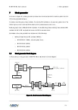
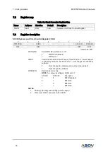


10. Timer0/1/2/3
MC97F6108A User’s manual
82
10
Timer0/1/2/3
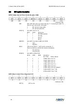
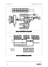
A 16-bit timer0/1/2/3 consists of multiplexer, timer0/1/2/3 data register high/low, timer0/1/2/3 register
high/low and timer0/1/2/3 mode register, PWM0/1/2/3 duty register high/low and PWM0/1/2/3 period
register high/low (TxDRH, TxDRL, TxH, TxL, TxCR, TxCR1, PWMxDRH, PWMxDRL, PWMxPRL,
PWMxPRH, x=0/1/2/3).
A 16-bit timer0/1/2/3 can be clocked by internal or external clock source (TxEC0 and TxEC1), the
divided clock of the main clock selected from prescaler output.
Timer0/1/2/3 operates in one of the following modes:
16-bit timer/counter mode
16-bit capture mode
16-bit PWM output mode
The timer/counter0/1/2/3 uses an internal clock or an external clock (TxEC0 and TxEC1) as an input
clock source. The clock sources are introduced below, and one is selected by clock selection logic
which is controlled by clock selection bits (TxCK[2:0]). Also, TxEC0 and TxEC1 can be selected by
event count and external interrupt selection bits (TxIN[2:0]).
TIMER0/1/2/3 clock source: fx/1, 4, 8, 16, 64, 256, 1024, 2048, TxEC0 and TxEC1
In capture mode, the data is captured into input capture data register (CDRxH/CDRxL) by TxCAP0/1/2.
In addition, Timer0/1/2/3 outputs PWM waveform through TxO/PWMx port in the PWM mode.
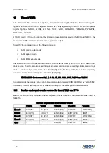
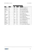
10.1
Capture and event counter source for timer0/1/2/3 and PPG
Each of timer0/1/2/3 and PPG has different capture sources and event counter sources as shown in
Table 13.
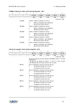
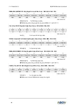
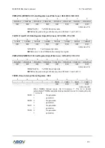
Table 13. Capture and Event Counter Source
TxEC0
TxEC1
TxCAP0
TxCAP1
TxCAP2
Timer 0
CPOUT0
EC1(P01)
EINT0(P02)
CMP0IF
EINT2(P04)
Timer 1
EC0(P10)
CPOUT1
EINT0(P02)
EINT1(P03)
CMP1IF
Timer 2
CPOUT2
EC1(P01)
EINT0(P02)
CMP2IF
EINT2(P04)
Timer 3
EC0(P10)
CPOUT3
EINT0(P02)
EINT1(P03)
CMP3IF
PPG
-
-
CMP3IF
CMP1IF
CMP4IF