A96G140/A96G148/A96A148 User’s manual
15. USI
181
15.20
USIn I2C block diagram
Receive Shift Register
(RXSR)
Transmit Shift Register
(TXSR)
I
N
T
E
R
N
A
L
B
U
S
L
I
N
E
SCLK
(fx: System clock)
SDAn
SCLn
USInDR, (Rx)
VSS
N-ch
VSS
N-ch
SCLn Out
Controller
SDAn In/Out
Controller
SDA Hold Time Register
USInSDHR
SCL Low Period Register
USInSCLR
SCL High Period Register
USInSCHR
Time Generator
And
Time Controller
USInDR, (Tx)
Slave Address Register
USInSAR
General Call And
Address Detector
USInGCE
STOP/START
Condition Generator
STOPCn
STARTCn
ACK Signal
Generator
ACKnEN
RXACKn, GCALLn,
TENDn, STOPDn,
SSELn, MLOSTn,
BUSYn, TMODEn
Interrupt
Generator
To interrupt
block
IICnIFR
IICnIE
NOTE
: When the USIn block is an I2C mode and the corresponding port is a sub-function for SCLn/SDAn pin,
The SCLn/SDAn pins are automatically set to the N-channel open-drain outputs and the input latch is
read in the case of reading the pins. The corresponding pull-up resistor is determined by the control
register.
Figure 100. USIn I2C Block Diagram
15.21
Register map
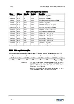
Table 31. USI Register Map
Name
Address
Direction
Default
Description
USI0BD
E3H
R/W
FFH
USI0 Baud Rate Generation Register
USI0DR
E5H
R/W
00H
USI0 Data Register
USI0SDHR E4H
R/W
01H
USI0 SDA Hold Time Register
USI0SCHR E7H
R/W
3FH
USI0 SCL High Period Register
USI0SCLR E6H
R/W
3FH
USI0 SCL Low Period Register
USI0SAR
DDH
R/W
00H
USI0 Slave Address Register
USI0CR1
D9H
R/W
00H
USI0 Control Register 1
USI0CR2
DAH
R/W
00H
USI0 Control Register 2
USI0CR3
DBH
R/W
00H
USI0 Control Register 3
USI0CR4
DCH
R/W
00H
USI0 Control Register 4


