background image

FM680 User Manual 


r1.7


FM680 


            www.abaco.com 

Page 9 of 32


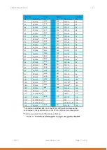
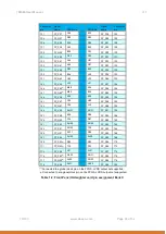
INTER_FPGA_IO12 

13  PN4_V 

L17 

21  BLAST0_VIO 

BA25 

INTER_FPGA_IO13 

13  PN4_V 

L16 

21  BLAST0_VIO 

BA26 

INTER_FPGA_IO14 

13  PN4_V 

G18 

21  BLAST0_VIO 

BB26 

INTER_FPGA_IO15 

13  PN4_V 

H17 

21  BLAST0_VIO 

BB27 

INTER_FPGA_CLK_A_to_Bn 

4  2V5 

V7 

34  BLAST0_VIO 

AY13 

INTER_FPGA_CLK_A_to_Bp 

4  2V5 

V8 

34  BLAST0_VIO 

AY14 

INTER_FPGA_CLK_B_to_An 

4  2V5 

P9 

34  BLAST0_VIO 

AP12 

INTER_FPGA_CLK_B_to_Ap 

4  2V5 

R9 

34  BLAST0_VIO 

AP11 


5.3  PCI-express architecture 

The Virtex-5 device is connected to the XMC connector (P15) and offers a PCI Express® 
Endpoint block integrated in the FPGA. The endpoint will support a 4 lanes generation 1 PCI-
express bus.  

A PCI express switch is used to optionally route the 4 lanes from the P15 connector to the 
Virtex-6 device instead of the Virtex-5 device. The remaining 4 transceiver lanes on the P15 
connector are routed to the Virtex-6 device as well. This makes it possible to have an 8 lanes 
generation 1 PCI-express bus connecting to the Virtex-6 device. If this option is selected the 
4 lanes connection towards the Virtex-5 device is not available.  


The standard reference design has the PCI Express connection towards the Virtex-5 FPGA. 
Abaco can provide a reference design for the 8-lanes connection to the Virtex-6 FPGA. 
Please consult with your sales contact for more details. 


The following performances have been recorded with the FM680 transferring data on the bus 
using the standard Abaco PCIe interface design: 


PCIe 1 lane: 150Mbytes/s sustained 


PCIe 4 lanes: 600Mbytes/s sustained 


PCIe 8 lanes: 800Mbytes/s sustained 


Higher performance transfers are possible but will require modifications to the PCIe interface 
design. Please consult with your sales contact for more details. 


Furthermore the VITA 42.3 standard defines an optional P16 connector which can carry an 
additional 8 lanes of high speed signaling. All these lanes are routed to the Virtex-6 device 
directly. An overview of the PCI-express subsystem is shown in Figure 3. 

Содержание FM680

Страница 1: ...1 of 32 FM680 User Manual for Virtex 6 XMC card Abaco Systems USA Support Portal This document is the property of Abaco Systems and may not be copied nor communicated to a third party without the written permission of Abaco Systems Abaco Systems 2009 ...

Страница 2: ...agram Added detailed description for the XMC connector usage Removed reference to emcore connector and the QTE connector Updated PCIexpress connection diagram Added location images for LEDs and switch Added table to describe interFPGA pinout NA NA NA 2012 07 11 r1 6 Updated chapter 9 3 to add more detail with regards to the front panel optical transceivers NA NA NA 2012 08 28 r1 7 Corrected table ...

Страница 3: ...or 12 5 6 Pn4 user I O connector 13 5 7 Serial FLASH 14 5 8 BLAST sites 14 5 9 External IO interfaces 15 5 9 1 Front Panel daughter card 15 5 9 2 Power connection to the front panel I O daughter card 19 5 9 3 Front Panel optical transceivers 19 5 9 4 Optical transceiver MGT Reference Clock 21 5 10 FPGA LED 21 5 11 FPGA configuration 23 5 11 1 Flash storage 23 5 11 2 CPLD device 23 5 11 3 JTAG 25 5...

Страница 4: ...Voltage Differential Signaling MGT Multi Gigabit Transceiver MSB Most Significant Bit s PCB Printed Circuit Board PCI Peripheral Component Interconnect PCI e PCI Express PLL Phase Locked Loop PMC PCI Mezzanine Card QDR Quadruple Data rate SDRAM Synchronous Dynamic Random Access memory SRAM Synchronous Random Access memory Table 1 Glossary 2 Related Documents IEEE Std 1386 1 2001 IEEE Standard Phys...

Страница 5: ...in Figure 1 Virtex 6 XC6VLX240T XC6VLX550T XC6VSX315T XC6VSX475T User I O clocks Configuration circuit and JTAG Flash 512Mbit LED x4 LED x4 Optional battery for IP encryption key 8 single ended to from Pn4 1 Pn4 Front Panel 180 pin QTH connector on side 1 and on side 2 facing inward or 4 optical tranceivers 2 5 Gb s Optionally conduction cooled Pn5 PCI Express VITA 42 3 PCI express end point BLAST...

Страница 6: ... Started Guide 5 Design 5 1 FPGA devices The Virtex 5 and Virtex 6 FPGA devices interface to the various resources on the FM680 as shown on Figure 1 They also interconnect to each other via 58 general purpose pins including 4 clock pins 2 pairs one in each direction 100Ω terminated A 16 bits single ended bus is also available between the two FPGA devices for communication with the Pn4 bus or gener...

Страница 7: ...T0_VIO AU13 INTER_FPGA1 1 BLAST0_VIO A6 34 BLAST0_VIO AR13 INTER_FPGA2 1 BLAST0_VIO E9 34 BLAST0_VIO AP13 INTER_FPGA3 1 BLAST0_VIO D8 34 BLAST0_VIO AN13 INTER_FPGA4 1 BLAST0_VIO D10 34 BLAST0_VIO AM13 INTER_FPGA5 1 BLAST0_VIO D9 33 BLAST0_VIO AK14 INTER_FPGA6 1 BLAST0_VIO C8 33 BLAST0_VIO AL14 INTER_FPGA7 1 BLAST0_VIO C7 33 BLAST0_VIO AM14 INTER_FPGA8 1 BLAST0_VIO B9 34 BLAST0_VIO AN14 INTER_FPGA9...

Страница 8: ...6 33 BLAST0_VIO AJ17 INTER_FPGA42 11 BLAST0_VIO G16 33 BLAST0_VIO AJ18 INTER_FPGA43 11 BLAST0_VIO A18 33 BLAST0_VIO AK18 INTER_FPGA44 11 BLAST0_VIO A17 33 BLAST0_VIO AN18 INTER_FPGA45 11 BLAST0_VIO E17 33 BLAST0_VIO AP18 INTER_FPGA46 11 BLAST0_VIO E16 33 BLAST0_VIO AR18 INTER_FPGA47 11 BLAST0_VIO C17 33 BLAST0_VIO AU18 INTER_FPGA48 11 BLAST0_VIO F17 33 BLAST0_VIO AV18 INTER_FPGA49 11 BLAST0_VIO D1...

Страница 9: ...vice as well This makes it possible to have an 8 lanes generation 1 PCI express bus connecting to the Virtex 6 device If this option is selected the 4 lanes connection towards the Virtex 5 device is not available The standard reference design has the PCI Express connection towards the Virtex 5 FPGA Abaco can provide a reference design for the 8 lanes connection to the Virtex 6 FPGA Please consult ...

Страница 10: ...ET0x 3 PER0x 4 PET0x 4 PER0x 5 PET0x 5 PER0x 6 PET0x 6 PER0x 7 PET0x 7 MGT_112_0 MGT_112_1 MGT_112_2 MGT_112_3 MGTREFCLK_112_0 MGT_113_0 MGT_113_1 MGT_113_2 MGT_113_3 MGT_114_0 MGT_114_1 MGT_114_2 MGT_114_3 MGT_115_0 MGT_115_1 MGT_115_2 MGT_115_3 PER1x 0 PET1x 0 PER1x 1 PET1x 1 PER1x 2 PET1x 2 PER0x 3 PET0x 3 PER0x 4 PET1x 4 PER1x 5 PET1x 5 PER1x 6 PET1x 6 PER1x 7 PET1x 7 RefCLK MGTREFCLK_114_0 MG...

Страница 11: ... 17 PER0p6 PER0n6 RFU PER0p7 PER0n7 RFU 18 GND GND RFU GND GND RFU 19 REFCLK 0 REFCLK 0 RFU WAKE ROOT0 RFU Table 4 XMC P15 connections FPGA Pin Name Description FPGA Bank DIR XMC P15 Pin Number Pin Name V5_U8 PCIexpress reset input 4 I F2 MRSTI n a Connected to GND n a O F12 MPRESENT n a Not connected n a O C11 MBIST n a Conencted to TDO n a I C8 TDI n a Conencted to TDI n a O C10 TDO n a VPOWER i...

Страница 12: ...T1p5 PET1n5 UD 6 GND GND UD GND GND UD 7 PET1p6 PET1n6 UD PET1p7 PET1n7 UD 8 GND GND UD GND GND UD 9 RFU RFU UD RFU RFU UD 10 GND GND UD GND GND UD 11 PER1p0 PER1n0 UD PER1p1 PER1n1 UD 12 GND GND UD GND GND UD 13 PER1p2 PER1n2 UD PER1p3 PER1n3 UD 14 GND GND UD GND GND UD 15 PER1p4 PER1n4 UD PER1p5 PER1n5 UD 16 GND GND UD GND GND UD 17 PER1p6 PER1n6 UD PER1p7 PER1n7 UD 18 GND GND UD GND GND UD 19 R...

Страница 13: ...N11 Pn4_IO21 22 23 Pn4_IO22 T17 T16 Pn4_IO23 24 25 Pn4_IO24 T12 R12 Pn4_IO25 26 27 Pn4_IO26 T18 U18 Pn4_IO27 28 29 Pn4_IO28 P10 N10 Pn4_IO29 30 31 Pn4_IO30 U16 U15 Pn4_IO31 32 33 Pn4_IO32 V18 V17 Pn4_IO33 34 35 Pn4_IO34 R10 R11 Pn4_IO35 36 37 Pn4_IO36 V16 V15 Pn4_IO37 38 39 Pn4_IO38 T11 U11 Pn4_IO39 40 41 Pn4_IO40 R14 T14 Pn4_IO41 42 43 Pn4_IO42 V10 U10 Pn4_IO43 44 45 Pn4_IO44 U14 T13 Pn4_IO45 46 ...

Страница 14: ...h device to the Virtex 6 are passed through a level translator SN74AVC4T245 5 8 BLAST sites Thanks to the availability of 5 BLAST sites a wide variety of memory and processing modules can be connected to the Virtex 6 device For each BLAST site it is possible to choose from the list of available BLAST modules For more information about the available BLASTs on the FM680 please consult the following ...

Страница 15: ...ical transceivers The Virtex 6 device interfaces to a 180 pin connector placed in the Front panel I O area on both side 1 of the PCB It serves as a base for a daughter card and offers I O diversity to the FM680 PMC The FPGA I O banks are powered either by 1 8V or 2 5V via a large 0 ohms resistor 2 5V is the default if not specified otherwise at the time of order Using the Xilinx DCI termination op...

Страница 16: ... FP_N9 28 29 FP_X8 C15 D15 FP_X9 30 31 FP_P10 2 M14 M16 FP_P11 32 33 FP_N10 2 N14 N15 FP_N11 34 35 FP_X10 H14 G13 FP_X11 36 37 FP_P12 A17 L16 FP_P13 38 39 FP_N12 B17 L15 FP_N13 40 41 FP_X12 J16 H16 FP_X13 42 43 FP_P14 D18 K17 FP_P15 44 45 FP_N14 C18 J17 FP_N15 46 47 FP_X14 M18 N18 FP_X15 48 49 FP_P16 2 N16 L12 FP_P17 1 50 51 FP_N16 2 P16 M12 FP_N17 1 52 53 FP_X16 K18 J18 FP_X17 54 55 FP_P18 1 E14 ...

Страница 17: ... F21 E22 FP_X29 90 91 FP_P30 E24 C21 FP_P31 92 93 FP_N30 E23 D21 FP_N31 94 95 FP_X30 H20 G21 FP_X31 96 97 FP_P32 K20 A22 FP_P33 98 99 FP_N32 L20 A21 FP_N33 100 101 FP_X32 D23 D22 FP_X33 102 103 FP_P34 B21 J22 FP_P35 2 104 105 FP_N34 A20 K22 FP_N35 2 106 107 FP_X34 J20 H19 FP_X35 108 109 FP_P36 2 L22 L21 FP_N36 2 110 111 3 3V 2 5V 1 8V Vbatt 3 112 113 FP_X36 K19 L19 FP_X37 114 115 3 3V 2 5V 1 8V 0 ...

Страница 18: ...5 2 M29 B36 FP_N46 148 149 FP_X48 K29 K30 FP_X49 150 151 FP_P47 C35 H30 FP_P48 152 153 FP_N47 C36 J30 FP_N48 154 155 FP_X50 AH31 AG31 FP_X51 156 157 FP_P49 E34 D36 FP_P50 158 159 FP_N49 F34 D37 FP_N50 160 161 FP_X52 AH29 AG29 FP_X53 162 163 FP_P51 AG32 T30 FP_P52 164 165 FP_N51 AF31 R30 FP_N52 166 167 FP_X54 AH30 AJ30 FP_X55 168 169 FP_P53 2 R32 N33 FP_P54 170 171 FP_N53 2 T32 P33 FP_N54 172 173 F...

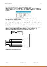
Страница 19: ...vers LTP ST11M are available on the FM680 in the front panel area They are connected to the MGT I Os of the Virtex 6 Infiniband protocols as well as Gigabit Ethernet and Fibre channel sFPDP can be implemented over the transceivers Lower rate optical transceivers 2 125 GB s and 1 0625 GB s are available in the same form factor The Figure 4 shows the block diagram of the optical transceivers on the ...

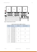
Страница 20: ...MGT connections FPGA Pin Net Name MGT Block Optical transceiver K4 MGT_FP_RXp3 116_3 OT3 K3 MGT_FP_TXp3 J6 MGT_FP_RXn3 J5 MGT_FP_RXp3 L2 MGT_FP_RXp2 116_2 OT2 L1 MGT_FP_TXp2 L6 MGT_FP_RXn2 L5 MGT_FP_RXp2 M4 MGT_FP_RXp1 116_1 OT1 M3 MGT_FP_TXp1 N6 MGT_FP_RXn1 N5 MGT_FP_RXp1 N2 MGT_FP_RXp0 116_0 OT0 N1 MGT_FP_TXp0 P8 MGT_FP_RXn0 P7 MGT_FP_RXp0 ...

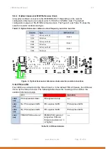
Страница 21: ...up default FSEL1 R494 Pull down R292 Pull up default FSEL2 R293 Pull down 518 510 R294 R494 R292 R293 Figure 6 Optical transceiver reference clock selection resistors locations 5 10 FPGA LED Four LEDs are connected to the Virtex 5 device In the default FPGA firmware the LEDs are driven by the Virtex 5 device The following table shows the meaning of the LEDs in the standard reference design OFF ON ...

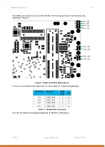
Страница 22: ..._LED3 FPGA_LED1 FPGA_LED0 CPLD_LED3 CPLD_LED2 CPLD_LED0 CPLD_LED1 Figure 7 FPGA and CPLD LED locations To turn on a LED drive the signal low To turn a LED off make the signal high FPGA Pin Net Name FPGA Bank DIR C13 FPGA_LED0 11 O C16 FPGA_LED1 11 O D17 FPGA_LED2 11 O B11 FPGA_LED3 11 O Table 17 FPGA LED connections The I O standard to be assigned depends on BLAST configuration ...

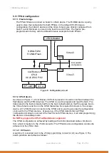
Страница 23: ...rface between the flash device and the FPGA devices The CPLD is used to program and read the flash The data stored in the flash is transferred from the host motherboard via the PCI express bus to the Virtex 5 device and then to the CPLD that writes the required bit stream to the storage device A 31 25 MHz clock connects to the CPLD and is used to generate the configuration clock sent to the FPGA d...

Страница 24: ...rtex 5 device safety configuration loaded from the flash at power up To be used only if the Virtex 5 device cannot be configured or does not perform properly with the switch in the OFF position Sw2 Reserved should be OFF Sw3 Reserved should be ON Sw4 Reserved should be OFF Table 18 Switch description 5 11 2 2 LED and board status Four LEDs connect to the CPLD and give information about the board s...

Страница 25: ...ror detected CRC error Presumably a wrong or corrupted FPGA bit stream has been written to the flash Once on this LED remains on n a Table 19 LED board status The LEDs are located on side 2 of the PCB in the front panel area Their locations are depicted in Figure 7 5 11 3 JTAG A JTAG connector is available on the FM680 for configuration purposes The JTAG can also be used to debug the FPGA design w...

Страница 26: ...ffers an efficient distribution of low jitter clocks Both FPGA devices receive a low jitter 125MHz clock A low jitter programmable clock able to generate frequencies from 62 5MHz to 255 5MHz in steps of 0 5MHz is also available This clock management approach ensures maximum flexibility to efficiently implement multi clock domains algorithms and use the memory devices at different frequencies Both ...

Страница 27: ...opriate voltage rails for the different devices and interfaces present on board The FM680 power consumption depends mainly on the FPGA devices work load By using high efficiency power converters all care has been taken to ensure that power consumption will remain as low as possible for any given algorithm After power up the FM680 typically consumes 6 Watts of power For precise power measurements i...

Страница 28: ... 0V 10 A Virtex 5 device core 1 0V 2 A BLAST core and IO Virtex 6 I O banks 1 8V 6A Virtex 5 device I O bank connected to the front panel daughter card 0 9 1 0 1 8 2 5 3 3V A front Panel I O daughter card 5V 1A Front Panel IO daughter card 3V3 3A Front Panel IO daughter card 12V 1A Front Panel IO daughter card 12V 1A MGT power supply 1 0V 1 2V 2 5V 2 0A 2 5A 0 01A respectively Table 22 Power suppl...

Страница 29: ...v5 TPS74401 1v8 1v0 1v2 to 1v0 TPS74401 1V2 5V 2V5 1v8 to 1v2 TPS74401 5v to 1v0 EN5396QI V6 5A V5 1A 12v to 5v0 LTC3605 Iout 6A XMC VPWR XMC XMC FET 5V0 ENABLE CONTROL Figure 12 Power supply An ADT7411 device is used to monitor the power on the different voltage rails as well as the temperature The ADT7411 data are constantly passed to the Virtex 6 device Measurements can be accessed from the hos...

Страница 30: ...will result in damaging the board The external power connector is of type Molex 43045 1021 Each circuit can carry a maximum current of 5A The connector pin assignment is as follows Pin Signal Signal Pin 1 3 3V 3 3V 2 3 5V 5V 4 5 GND GND 6 7 GND GND 8 9 12V 12V 10 Table 23 External power connector pin assignment WARNING UNREGULATED UNPROTECTED EXTERNAL POWER SUPPLY CONNECTION This board is designed...

Страница 31: ... PMC The FM680 is compliant to ANSI VITA 20 2001 standard for conduction cooled PMC 8 Safety This module presents no hazard to the user 9 EMC This module is designed to operate from within an enclosed host system which is build to provide EMC shielding Operation within the EU EMC guidelines is not guaranteed unless it is installed within an adequate host system This module is protected from damage...

Страница 32: ... as specifically identified in the products official documentation Any modification to hardware including but not limited to removing of components soldering or other material changes to in part or in whole to the PCM and or its components will immediately invalidate and make void any warranty or extended support if any Further and changes or modifications to software and or firmware supplied with...

Отзывы: