1
SLLU216 – July 2019
Copyright © 2019, Texas Instruments Incorporated
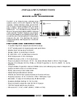
SPI to CAN FD SBC + LIN Transceiver BoosterPack User's Guide
User's Guide
SLLU216 – July 2019
SPI to CAN FD SBC + LIN Transceiver BoosterPack User's
Guide
The SPI to CAN FD SBC + LIN BoosterPack™ features the TCAN4550-Q1 CAN FD controller with
integrated transceiver providing microcontrollers without an integrated CAN FD controller, or those
needing additional channels, access to CAN FD applications through a SPI interface. LIN applications can
also be developed using the TLIN2029-Q1 fault protected LIN transceiver and the MCU UART port
making this BoosterPack an ideal starting point for any CAN FD or LIN system.
spacer
Contents
1
Introduction
...................................................................................................................
1.1
Features
..............................................................................................................
2
Hardware description
.......................................................................................................
2.1
Power
................................................................................................................
2.2
CAN
..................................................................................................................
2.3
LIN
....................................................................................................................
2.4
MCU interface (SPI/GPIO)
........................................................................................
3
Firmware
....................................................................................................................
3.1
CAN / CAN FD Controller Configuration
.......................................................................
3.2
Sending and Receiving CAN Messages
.......................................................................
3.3
Performance Optimization
........................................................................................
3.4
Microcontroller Abstraction
.......................................................................................
4
Board Layout
................................................................................................................
5
Schematic and Bill of Materials
...........................................................................................
5.1
Schematic
..........................................................................................................
5.2
Bill of Materials
....................................................................................................
List of Figures
1
BOOSTXL-CANFN-LIN
.....................................................................................................
2
Power components and features
.........................................................................................
3
CAN bus components and features
......................................................................................
4
LIN bus components and features
........................................................................................
5
MCU interface components and features
...............................................................................
6
Pinout
.......................................................................................................................
7
Nominal bit time
...........................................................................................................
8
Visual representation of MRAM allocation
.............................................................................
9
AutoSAR Abstraction Layers
.............................................................................................
10
Microcontroller Abstraction
...............................................................................................
11
32-bit SPI read or write example
........................................................................................
12
SPI packet breakdown
....................................................................................................
13
Multi-word SPI packet example
..........................................................................................
14
BoosterPack Top
...........................................................................................................
15
BoosterPack Bottom
.......................................................................................................
16
BoosterPack Schematic
...................................................................................................