background image

SERVICE MANUAL

AEP Model

UK Model

Russian Model

PORTABLE CD/DVD PLAYER

DVP-FX850

RMT-D183

SPECIFICATIONS

System

Laser: Semiconductor laser
Signal format system: PAL (NTSC)

Audio characteristics

Frequency response: DVD VIDEO (PCM 

48 kHz): 20 Hz to 22 kHz/
CD: 20 Hz to 20 kHz

Harmonic distortion: 0.01 %
Dynamic range: DVD VIDEO: 90 dB/

CD: 90 dB

Wow and flutter: Less than detected value 

(

±

0.001% W PEAK)

Inputs/Outputs

VIDEO (video input/output): 

Minijack (1)
Output 1.0 Vp-p/75 ohms

AUDIO (audio input/output)/OPTICAL 

OUT (optical output):
Stereo minijack/optical minijack 
combined (1)
Output 2.0 Vrms/47 kilohms
Recommended load impedance over 
47 kilohms

PHONES (headphones) A/B:

Stereo minijack (2)

Liquid Crystal Display

Panel size: 8 inches wide (diagonal)
Driving system: TFT active matrix
Resolution: 800 

×

 480 (effective pixel rate: 

more than 99.99%)

General

Power requirements:

DC 9.5 V (AC Adaptor/Car battery 
adaptor)
DC 7.4 V (Battery pack)

Power consumption (DVD VIDEO 

Playback):
23 W (when used with a battery pack) 
8.5 W (when used without a battery pack, 
with a headphone) 

Dimensions (approx.):

226.2 

×

 32.3 

×

 165.3 mm (width/height/

depth) incl. projecting parts

Mass (approx.): 1.045 kg
Operating temperature: 5

°

C to 35

°

Operating humidity: 25 % to 80 %
AC Adaptor: 100-240 V AC, 50/60 Hz
Car Battery Adaptor: 12 V DC

Supplied accessories

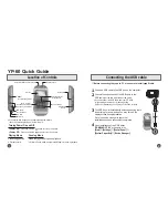
• Audio/video cord (mini plug 

×

 2 

y

 phono

  plug 

×

 3) (1)

• Mains lead (1)
• AC adaptor (AC-FX150) (1)
• Car battery adaptor (DCC-FX150) (1)
• Battery pack (NP-FX110) (1)
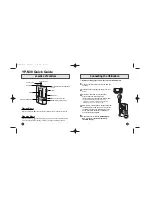
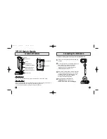
• Remote (with battery) (1)
• Carry case (1)

Desing and specifications are subject to 
change without notice.

Summary of Contents for DVP-FX850

Page 1: ... minijack 2 Liquid Crystal Display Panel size 8 inches wide diagonal Driving system TFT active matrix Resolution 800 480 effective pixel rate more than 99 99 General Power requirements DC 9 5 V AC Adaptor Car battery adaptor DC 7 4 V Battery pack Power consumption DVD VIDEO Playback 23 W when used with a battery pack 8 5 W when used without a battery pack with a headphone Dimensions approx 226 2 3...

Page 2: ...aded solder melts at a temperature about 40 C higher than ordinary solder Ordinary soldering irons can be used but the iron tip has to be applied to the solder joint for a slightly longer time Soldering irons using a temperature regulator should be set to about 350 C Caution The printed pattern copper foil may peel away if the heated tip is applied for too long so be careful Strong viscosity Unlea...

Page 3: ...IO OUT 4 13 4 7 IR KB 4 15 4 8 T CON 4 17 4 9 USB 4 19 5 PRINTED WIRING BOARDS 5 1 Circuit Boards Location 5 1 5 2 MAIN Board 5 3 5 3 DRIVER Board 5 7 5 4 USB Board 5 9 6 WAVEFORMS AND CIRCUIT VOLTAGE 6 1 Waveforms 6 1 6 2 Circuit Voltage Chart 6 5 7 IC PIN FUNCTION DESCRIPTION 7 1 MPEG DSP RF Pin Function MAIN Board U7 MT1389HD 7 1 7 2 FRONT MICOM Pin Function MAIN Board U3 Z8F0822 7 7 8 ELECTRIC...

Page 4: ... 4 MEMO ...

Page 5: ... while listening to a section with very low level inputs or no audio signals If you do the speakers may be damaged when a peak level section is played On headphones Preventing hearing damage Avoid using headphones at high volumes Hearing experts advice against continuous loud and extended play If you experience a ringing in your ears reduce the volume or discontinue use Showing consideration for o...

Page 6: ... the Remote When operating point it at the remote sensor on the player To replace the remote control battery Insert a lithium battery CR2025 matching the 3 and ends of the battery 1 Pull out the battery holder 2 while pressing the lock lever 1 2 Remove the old battery 3 Insert the new battery in the battery holder with the 3 side up and then push the holder fully Notes Do not expose the remote sen...

Page 7: ...cars grounded positively z Hint If the car adaptor interferes with car operation use a commercial cigarette lighter extension cord Notes Do not use the car adaptor if it has been dropped or damaged Arrange the cord so as not to interfere with the driver Also do not place the LCD panel where the driver can watch If the picture is not clear keep the player away from the car battery adaptor Use the c...

Page 8: ... use C c on the remote 1 2 3 4 5 6 7 8 0 9 H x 1 2 3 4 5 6 7 8 0 9 TOP MENU C X x c ENTER MENU Number buttons continued 18 Changing the sound When playing a DVD VIDEO recorded in multiple audio formats PCM Dolby Digital or DTS you can change the audio format If the DVD VIDEO is recorded with multilingual tracks you can also change the language With CDs or VIDEO CDs you can select the sound from ei...

Page 9: ... search without displaying the control menu See page 23 for details 1 2 3 4 5 6 7 8 0 9 Number buttons DISPLAY C X x c ENTER O Menu Title Chapter Audio Subtitle 02 07 03 20 02 2CH DOLBY DIGITAL English 01 English Title Elapsed 00 12 01 Current playback settings Items Elapsed or remaining time Battery status continued 22 See page 23 for details about using direct search for a CD or VIDEO CD Notes T...

Page 10: ...Doing so may cause data corruption or loss of data The access indicator on some USB devices may keep flashing even after the data is transferred USB devices which can connect to the player are flash memory and multiple card reader Other devices digital still camera USB hub etc cannot be connected When an incompatible device is connected Cannot recognise the connected device appears indicating that...

Page 11: ...video file 1 Press X x to select an album on the list and press ENTER A list of files in the album appears To go to the next or previous page press or To return to the list of albums press X x to select and press ENTER 2 Press X x to select the file you want to play and press ENTER Playback starts from the selected file To go to the next or previous DivX video file Press or To locate a point quick...

Page 12: ...utomatically displays a wide picture on the entire screen and cuts off the portions that do not fit 4 3 Letter Box Select this when you connect a 4 3 screen TV Displays a wide picture with bands on the upper and lower portions of the screen 16 9 Select this when you connect a wide screen TV or a TV with a wide mode function ENTER RETURN General Setup TV Display Angle Mark 16 9 On On On Screen Save...

Page 13: ...therefore first set the password in the set up Changing the password 1 Press X x to select Password in the Parental Control setting display and press ENTER 2 Select Change and press ENTER The display for entering the password appears 3 Enter your current 6 digit password in the Old Password box 4 Enter your new 6 digit password in the New Password box 5 Enter your new 6 digit password once again i...

Page 14: ... sound will come out when you select Stereo 1 Left 1 or Right 1 Re connect the connecting cord securely The connecting cord is damaged The player is connected to the wrong input jack on the amplifier receiver page 40 The amplifier receiver input is not correctly set If the audio signal does not come through the OPTICAL OUT jack check the audio settings page 36 The sound volume is low The sound vol...

Page 15: ...system Image standards for digital cameras regulated by JEITA Japan Electronics and Information Technology Industries Association 45 Additional Information Notes Change the extension to jpg for files with jpe or jpeg extension The player will play any data with the extension MP3 JPG or JPEG even if they are not in MP3 or JPEG format Playing this data may generate a loud noise which could damage yo...

Page 16: ... 4 3 Letter Box 34 4 3 Pan Scan 34 A Album 45 Angle 19 Audio 18 36 Audio DRC 35 Audio Setup 35 B Batteries 9 C CD 7 15 Connecting 39 D DATA CD 6 31 44 DATA DVD 6 31 44 Digital output 35 Disc Menu 36 Display Playback Settings Display 21 Setup Display 33 DivX 30 31 Dolby Digital 18 36 DTS 18 36 DVD 6 15 DVD RW 6 DVD s menu 17 DVD RW 6 20 F Fast forward 23 Fast reverse 23 G General Setup 34 H Handlin...

Page 17: ...DVP FX850 8 four screws M2 5 11 3 two foot rubbers 1 two foot rubbers 4 two screws TS2 8 5 2 two screws TS2 8 5 9 bottom assy qg six screws TS2 4 5 qh MAIN board 0 connector qa connector qf screw TS2 4 5 6 six screws TS2 8 5 5 two screws TS2 8 5 7 open preve sheet qh screw TS2 4 5 qj USB board qs connector qd connector ...

Page 18: ...2 2 2 2 TRAVERSE 1 traverse 2 hinge cosmetic ...

Page 19: ...UPPER BLOCK 9 disc lid assy 3 damping support 2 two screws TS2 4 5 8 disc open supp 5 disc lid open spr bracket 7 two screws TS2 4 5 4 three screws TS2 4 5 1 two screws TS2 4 5 qa upper block 0 spring 6 spring ...

Page 20: ...ds 4 two screws TS1 7 4 4 two screws TS1 7 4 2 two screws TS1 7 4 5 two screws TS1 7 2 1 two screw pads 3 two screw pads qa hinge assy qg panel brace qh panel assy qk hinge brace 8 housing assy 0 connector 7 two connectors 9 connector qs three screws TS1 7 5 qs three screws TS1 7 5 qf two screws TS1 7 5 qj two screws TS1 7 2 5 ...

Page 21: ...OTE CONTROL AT24CXX I2C Bus KEYPAD Serial Data Audio DAC PCM1742KE Command Bus 4558 Audio Audio In Out In Audio AMP CVBS Out CVBS Out In DIGITAL VOLUME CONTROL CVBS In I2C Y C Out Head Phone SPEAKER Motor Driver Traverse SPINDLE MOTOR SLEDGE MOTOR OPU MST7915MA Servo Signal Servo Driver Signal Audio R Audio L APA2068 TV Set TV Set TV Set R G Signal B Timing Control Main Board PCB Servo DSP MPEG IC...

Page 22: ...DVP FX850 3 4E DVP FX850 MEMO ...

Page 23: ...KEY1 P_SW KEY2 4 3 2 1 KEY4 5 KEY5 6 KEY6 7 KEY7 8 KEY8 9 KEY9 10 KEY10 11 KEY11 12 KEY12 13 P_3V3 14 IR_IN 15 GND 16 SP1 17 SP2 SP3 SP4 18 19 20 NC 1 USB_SW 2 DVD_SW 3 USB_GND 4 6 7 8 9 USBP D USBM D USB_GND USB_GND USB_VCC 5 LGND LGND 2 1 DC_IN1 3 DC_IN1 4 LGND 5 LGND 6 5V_TFT 7 5V_TFT 8 5V_TFT 9 LGND 10 TFT_C 11 LGND 12 TFT_Y 13 LGND 14 CVBS_IN 15 LGND TFT_SCL TFT_IRQ LGND TFT_SDA 16 17 19 20 1...

Page 24: ...0 TFT_C 11 LGND 12 STFT_Y 13 LGND 14 CVBS_IN 15 LGND 16 TFT_SDA TFT_SCL TFT_IRQ LGND 17 18 19 20 VCOM 1 DGND 2 PNL_AVDD 3 V13 4 V12 5 V10 6 V7 7 V4 8 V1 9 PNL_RL 10 PNL_B0 11 PNL_B1 12 PNL_B2 13 PNL_B3 14 PNL_B4 15 PNL_B5 16 PNL_LD 17 PNL_STHR 18 PNL_DVDD 19 PNL_CLK 20 DGND 21 DGND 22 PNL_STHL 23 PNL_G0 24 PNL_G1 25 PNL_G2 26 PNL_G3 27 PNL_G4 28 DGND 30 PNL_G5 29 DGND 1 PNL_R0 2 PNL_R1 3 PNL_R2 4 ...

Page 25: ...8 RLS4148 NC 2 1 ADPTE ADPTE R50 3 3R R50 3 3R FB65 FB 100R 3A NC FB65 FB 100R 3A NC C4 0 1uF C4 0 1uF C55 0 1uF NC C55 0 1uF NC 2N3904 Q10 2N3904 Q10 1 2 3 CBCHE CBCHE Q45 Q45 AP2309GN NC 2 3 1 MUTE MUTE EC4 47uF 10V 5 0X5 4 EC4 47uF 10V 5 0X5 4 C52 0 01uF C52 0 01uF U2 MP1412 U2 MP1412 NC 1 BS 2 NC 3 IN 4 SW 5 GND 6 FB 7 Comp 8 EN 9 SS 10 R46 10K R46 10K D7 RLS4148 NC D7 RLS4148 NC 2 1 C43 0 1uF...

Page 26: ... IO_7 167 C6 IO_6 168 YUVCLK IO_8 166 Y0 IO_9 165 Y1 IO_10 164 Y2 IO_11 163 Y3 IO_12 162 Y4 IO_13 161 DVDD18 160 Y5 IO_14 159 Y6 IO_15 158 DVDD3 156 Y7 IO_16 157 RA4 155 RA5 154 RA6 153 RA7 152 RA8 151 RA9 150 DVSS 148 RA11 149 CKE 147 RCLK 146 DVDD3 145 RA3 144 RA2 143 RA1 141 DVDD18 142 RA0 140 RA10 139 BA1 138 BA0 137 RCS 136 CAS 134 RAS 135 RWE 133 DQM1 132 DVDD3 131 IO_18 130 HRFZC 249 IREF 2...

Page 27: ...64A VCC 1 DQ0 2 DQ1 4 VSSQ 12 DQ2 5 DQ3 7 VCCQ 9 DQ4 8 DQ5 10 VSSQ 46 DQ6 11 DQ7 13 DQML 15 WE 16 CAS 17 RAS 18 CS 19 A11 35 A10 AP 22 A0 23 A1 24 A2 25 A3 26 VCC 14 VSS 41 A4 29 A5 30 A6 31 A7 32 A8 33 A9 34 NC 36 CKE 37 CLK 38 DQMH 39 NC 40 VCCQ 43 DQ8 42 DQ9 44 VSSQ 52 DQ10 45 DQ11 47 VCCQ 49 DQ12 48 DQ13 50 DQ14 51 DQ15 53 VSS 54 BA0 A13 20 BA1 A12 21 VCCQ 3 VSSQ 6 VCC 27 VSS 28 R129 NC R129 N...

Page 28: ...A L25 1 8uH 50mA J10 A1002H00 20PB J10 A1002H00 20PB 1 2 3 4 5 6 7 8 9 10 11 12 13 14 15 16 17 18 19 20 FB24 FB 1500R 300mA 0603 FB24 FB 1500R 300mA 0603 C191 0 1uF C191 0 1uF 5VT 5VT C205 0 1uF C205 0 1uF C179 1000pF C179 1000pF FB23 FB 1500R 300mA 0603 FB23 FB 1500R 300mA 0603 VIDE VIDE SR1 SR1 TIRQ TIRQ L26 1 8uH 50mA L26 1 8uH 50mA C201 0 1uF C201 0 1uF DCIN1 DCIN1 R131 100K R131 100K FB22 FB ...

Page 29: ... 220uF 10V 8 0X10 2 C217 1uF 0805 C217 1uF 0805 D16 MM4148 D16 MM4148 2 1 D25 PESD5V0S1BB D25 PESD5V0S1BB 1 1 2 2 C220 100pF C220 100pF R260 NC R260 NC C219 150pF C219 150pF R197 10K R197 10K R169 68R R169 68R R255 R255 7 5K1 NC Q31 2N3904 Q31 2N3904 1 2 3 EC51 10uF 10V 4 0X5 4 EC51 10uF 10V 4 0X5 4 Q49 2N3904 Q49 2N3904 3 2 1 R174 15K 1 R174 15K 1 R253 1M NC R253 1M NC R207 1K R207 1K R183 39R R1...

Page 30: ...on key EVQWHA50K J1 5 direction key EVQWHA50K 1 1 2 2 3 3 4 4 5 5 6 6 7 7 KS_C6 KS_C6 D6 PESD5V0S1BB NC D6 PESD5V0S1BB NC 1 1 2 2 SPL1 SPL1 KS_R1 KS_R1 SW9 RETURN SPR1 SPR1 SW4 D7 PESD5V0S1BB NC D7 PESD5V0S1BB NC 1 1 2 2 C84 100p C84 100p C87 100p C87 100p R69 1 8R 1206 C73 0 1u C73 0 1u CN6 AO 1 AO 2 KS_R4 KS_R4 KS_R2 KS_R2 KS_R3 KS_R3 KS_C3 KS_C3 C72 100P R70 10R IR1 IR_D3P IR1 IR_D3P 1 2 3 SW1 ...

Page 31: ... 24 38 STHL 23 39 INV 22 40 GND6 21 41 DCLK 20 42 VCC 19 43 STHR 18 44 LD 17 45 B5 16 46 B4 15 47 B3 14 48 B2 13 49 B1 12 50 B0 11 51 R L 10 52 V1 9 53 V4 8 54 V7 7 55 V10 6 56 V12 5 57 V13 4 58 AVDD2 3 59 GND7 2 60 VCOM2 1 DGND 31 DGND 32 C76 C76 1000P H12 H2D2 H12 H2D2 C24 0 1u C24 0 1u R7 R 0805 9 0 SD4 SGL34 02 SD4 SGL34 02 1 2 C51 0 1u C51 0 1u R59 390R R59 390R C78 470p C78 470p 8 2u L3 8 2u...

Page 32: ... UD4 PESD5V0S1BB NC UD4 PESD5V0S1BB NC 1 1 2 2 BM BM UC6 NC UC6 NC UC5 NC UC5 NC UFB2 FB 100R 0603 UFB2 FB 100R 0603 UR5 15K D D UJ2 UB1112C C1608 FR 4 2 3 1 UJ2 UB1112C C1608 FR 3 2 1 4 5 6 UC4 10uF 16V USBS USBS UR6 15K UR6 15K VCC VCC D D USW USW UR3 33R UR3 33R UT1 ACM2012 900 2P NC UT1 ACM2012 900 2P NC 2 1 3 4 UJ1 CCHD1407RE 00012 UJ1 CCHD1407RE 00012 1 2 3 4 5 6 7 8 9 UC2 0 1uF UC2 0 1uF UR...

Page 33: ...DVP FX850 5 1 5 2 SECTION 5 PRINTED WIRING BOARDS 5 1 CIRCUIT BOARDS LOCATION DRIVER BOARD MAIN BOARD USB BOARD ...

Page 34: ... G 6 Q27 G 5 Q28 H 8 Q29 H 6 Q30 G 7 Q31 F 8 Q32 E 8 Q33 F 8 Q34 E 8 Q35 D 8 Q36 E 7 Q49 H 7 U3 H 5 U7 E 3 U10 F 5 U12 E 3 U13 B 5 U14 G 7 U17 G 6 U18 E 6 U19 H 6 U22 H 5 U23 H 6 Uses unleaded solder See page 5 1 for circuit boards location There are a few cases that the part isn t mounted in this model is printed on this diagram C D E F G H A 1 2 3 4 5 6 7 8 05 B MAIN BOARD SIDE A DISC COVER SWIT...

Page 35: ...8 D15 D 7 D23 H 6 Q1 A 8 Q4 A 8 Q6 A 8 Q9 G 5 Q10 G 5 Q11 G 5 Q12 A 7 Q22 C 3 Q26 H 6 Q39 G 3 Q40 G 3 Q44 H 3 Q45 G 4 Q46 G 4 Q47 H 6 Q48 H 5 U1 B 7 U2 B 7 U4 D 7 U5 C 7 U6 A 7 U8 G 3 U9 G 4 U11 E 5 C D E F G H A 1 2 3 4 5 6 7 8 05 B MAIN BOARD SIDE B DC IN 9V LINE SELECT OUT IN r VIDEO AUDIO PHONES PHONES VOLUME TO RECHARGEABLE BATTERY PACK ...

Page 36: ...T C A 1 2 3 4 5 6 7 8 9 10 11 12 05 B DRIVER BOARD SIDE B LCDMODE RETURN MENU DISPLAY x X H SW1 SW2 SW3 SW4 SW5 SW7 SW7 SW9 SW6 1 2 1 2 2 1 1 2 3 4 1 2 3 4 1 2 3 4 1 2 3 4 1 2 3 4 1 2 3 4 1 2 3 4 1 2 3 4 1 2 3 4 T R r t ENTER 1 2 1 2 1 2 1 2 1 2 1 2 1 2 1 2 DRIVER BOARD SIDE A CN1 A 11 CN2 B 5 CN3 B 6 CN5 A 11 CN6 A 1 CN7 A 3 D1 A 2 BD1 A 3 BD2 A 3 BD3 A 3 SD2 B 1 SD3 B 1 SD4 B 10 SD5 B 11 Q1 B 2 ...

Page 37: ...D 2 UD4 D 2 Uses unleaded solder See page 5 1 for circuit boards location There are a few cases that the part isn t mounted in this model is printed on this diagram C D E F G A 1 2 1 2 1 2 05 B USB BOARD SIDE A 1 2 1 2 C D E F G A 1 2 05 B USB BOARD SIDE B CD DVD Y USB USB 1 4 3 3 2 6 ...

Page 38: ...DVP FX850 5 12E DVP FX850 MEMO ...

Page 39: ... disc condition DMSO ECR U9 PIN9 TEO U7 PIN32 TRSO U8 PIN26 U U9 PIN7 V U9 PIN4 W U9 PIN2 Fig 6 1 Fig 6 2 Fig 6 3 Fig 6 4 TEO U10 PIN32 AUDIO OUT J12 PIN2 TRSO U8 PIN26 2 Tracking control related signal system checking cd 4 Audio output from IC L R 3 Tracking control related signal system checking dvd ...

Page 40: ... 6 4 5 Audio related signal DIN U18 PIN2 DIN 13 PIN10 SCKIN U18 PIN16 DIN U18 PIN3 Fig 6 5 Fig 6 6 Fig 6 7 Fig 6 8 Y FB19 C FB44 DVDRFIP U7 PIN6 6 Video output waveform CVBS 8 RF waveform 7 Video output waveform Y C ...

Page 41: ...912 3 273 223 1 621 1 622 24 3 267 3 255 74 0 027 1 638 124 1 095 1 177 174 3 263 0 224 1 622 1 625 25 2 809 2 747 75 0 026 0 026 125 1 29 0 955 175 3 263 3 273 225 1 591 1 591 26 2 073 1 763 76 0 025 0 022 126 1 064 1 146 176 3 263 3 273 226 2 101 1 591 27 0 0 77 0 008 2 01 127 0 805 0 804 177 0 3 273 227 1 823 1 601 28 2 779 2 705 78 0 008 0 024 128 0 852 1 004 178 0 0 228 1 739 1 607 29 2 03 2 ...

Page 42: ...052 0 044 25 0 27 1 418 25 2 179 1 982 25 3 3 3 262 3 0 0 3 0 204 2 52 3 1 544 1 539 26 0 271 1 526 26 0 025 0 26 2 932 2 744 4 0 3 765 4 1 373 1 369 4 0 0 27 3 267 3 264 27 0 0 27 0 073 3 261 5 0 0 5 0 241 1 37 5 3 266 3 261 28 0 0 28 0 023 0 28 0 134 1 388 6 0 0 6 0 241 1 369 6 4 881 4 828 29 0 27 1 002 29 1 881 1 564 7 0 3 767 7 0 102 2 512 7 2 447 2 435 30 0 337 1 029 30 0 307 0 393 8 0 0 8 0 ...

Page 43: ...t 23 LDO1 O Laser driver output 24 SVDD3 Analog power 3 3V 25 CSO O Positive main beam summing output 26 RFLVL O Negative main beam summing output 27 SGND Analog ground 28 V2REFO O Reference voltage 2 8V 29 V20 O Reference voltage 2 0V 30 VREFO O Reference voltage 1 4V 31 FEO O Focus error monitor output 32 TEO O Tracking error monitor output 33 TEZISLV O TE Slicing Level 34 OP_OUT O TP162 35 OP_I...

Page 44: ...roller address 15 69 HIGHA6 I O Microcontroller address 14 70 HIGHA5 I O Microcontroller address 13 71 HIGHA4 I O Microcontroller address 12 72 HIGHA3 I O Microcontroller address 11 73 HIGHA2 I O Microcontroller address 10 74 HIGHA1 I O Microcontroller address 9 75 IOA20 I O Flash address 20 IO 76 IOCS I O Flash chip select active low IO 77 IOA1 I O Microcontroller address 1 IO 78 IOOE I O Flash o...

Page 45: ...I O GPIO 113 RD7 I O DRAM data 7 114 RD6 I O DRAM data 6 115 RD5 I O DRAM data 5 116 RD4 I O DRAM data 4 117 RD3 I O DRAM data 3 118 DVDD3 3 3V power pin for internal 119 RD2 I O DRAM data 2 120 RD1 I O DRAM data 1 121 RD0 I O DRAM data 0 122 RD15 I O DRAM data 15 123 RD14 I O DRAM data 14 124 RD13 I O DRAM data 13 125 RD12 I O DRAM data 12 126 RD11 I O DRAM data 11 127 RD10 I O DRAM data 10 128 R...

Page 46: ...C bit 7 GPIO 168 C_6 IO_6 I O Digital Video output C bit 6 GPIO 169 C_5 IO_5 I O Digital Video output C bit 5 GPIO 170 DVDD3 3 3V power pin for internal 171 C_4 IO_4 I O Digital Video output C bit 4 GPIO 172 C_3 IO_3 I O Digital Video output C bit 3 GPIO 173 C_2 IO_2 I O Digital Video output C bit 2 GPIO 174 DVDD18 1 8V power pin for internal 175 C_1 IO_1 I O Digital Video output C bit 1 GPIO 176 ...

Page 47: ...rnal 214 ASDATA4 I O TP151 215 MC_DATA I O Inout PD SMT 216 SPDIF O SPDIF output 217 APLLVDD3 3 3V Power pin for audio clock circuitry 218 APLLCAP O APLL External 219 APLLVSS Ground pin for audio clock circuitry 220 ADACVSS2 Ground pin for AUDIO DAC circuitry 221 ADACVSS1 Ground pin for AUDIO DAC circuitry 222 ARF SW O AUDIO DAC Sub woofer channel output While internal AUDIO DAC not used GPIO 223 ...

Page 48: ...Analog 3 3V Power for ADC 245 ADCVSS Analog ground for ADC 246 RFVDD3 Analog Power 247 RFRPDC O RF ripple detect output 248 RFRPAC I RF ripple detect input through AC coupling 249 HRFZC I High frequency RF ripple zero crossing 250 CRTPLP O Defect level filter capacitor connecting 251 RFGND Analog Power 252 OSP O RF Offset cancellation capacitor connecting 253 OSN O RF Offset cancellation capacitor...

Page 49: ... 3 3V 9 PC5 MISO O MUTE 10 PC4 MOSI I Battery detect 11 PC3 SCK I AV IN SW 12 PC2 SS O CHARGE EN 13 PA0 T0IN I ADAPTER_DET 14 PA1 T0OUT O VOL_PWM 15 PA2 DE0 I LED2 CHARGE 16 PA3 CTS0 I IR_IN 17 PA4 RXD0 I O TXD 18 PA5 TXD0 I O RXD 19 PC1 T1OUT O SE 20 DBG I DBG 21 AVdd 3 3V 22 AVss Ground pin 23 VREF 3 3V 24 PB4 ANA4 O cb charge enable 25 PB3 ANA3 O S MUTE 26 PB2 ANA2 I AUDIO_DTC 27 PB1 ANA1 I LED...

Page 50: ...7 8E MEMO ...

Page 51: ...1 Checking Video Output Level Purpose This checks whether Video Output level satisfy the NTSC stan dard If it is not correct the brightness will be too large or small Mode Play Signal Check the Color bar 100 signal on DVD reference disc Measurement Point LINE OUT VIDEO connector 75 Ω terminated Measuring Instrument Oscilloscope Specification 1 00 0 05 Vp p Checking method 1 Confirm that the Video ...

Page 52: ...8 2E MEMO ...

Page 53: ...ce U4 Replace U6 Is U6 OK Replace D2 Replace adaptor Is battery OK Replace Q1 Is Q1 OK Replace battery AUDIO OUT ABNORMAL SPEAKER ABNORMAL Is S1 S2 OK Replace S1 S2 Replace U14 Replace U7 Replace speaker Is U14 OK Is speaker OK Check audio jack mode Check U19 Check U17 Check U18 Check signals from U7 MT1389 YES YES YES YES NO NO NO NO NO NO NO NO NO NO NO NO NO NO NO YES YES YES YES YES YES YES YE...

Page 54: ...nection of part Check traverse PICTURE ABNORMAL DISC ERROR Check video jack mode Check the disc Check disc Check the traverse Check traverse Check the SDRAM Refer to servo part Refer to servo part Check LC filter Check video signals from U7 MT1389 YES YES YES YES D Video out abnormal G Open close abnormal H Charging circuit E Picture abnormal F Disc error NO NO NO NO NO Refer to servo part ...

Page 55: ...ck CD DVD DSP output signal Check MPEG decoder input signal Is clock normal Check clock signal Check clock signal Does the audio signal output from MPEG decoder Does the audio sound output normally 2 MPEG Circuit NO NO NO YES YES YES YES YES OK OK MT1389HD MT1389HD OK OK NO YES NO NO NO YES NO NO Check CD DVD DSP output signal Check MPEG decoder input signal Check CD DVD DSP output signal Check MP...

Page 56: ...es IR1 work by testing waveform normally Is battery OK Check J3 on the mainboard Check IC MT1389 Replace IC MT1389 Replace IC MT1389 Replace battery Replace IR1 Check the buttons Is P_3V3 OK Do the U3 work normally Check power Replace U3 3 Front Circuit Dogotrpm key YES YES YES YES YES YES YES NO NO NO YES YES NO NO NO NO YES NO NO NO ...

Page 57: ...per TRSO signal on MT1389 TR TR out properly Check cable connection on pick up head Check the cable connection on pick up head Check the related circuit on MT1389 FO FO signal Check connection between MT1389 and pick up head Check the RF connection between J5 and MT1389 Proper DMSO signal on MT1389 Check the cable connection between spindle and main PCBA Check the related circuit on MT1389 RFL sig...

Page 58: ...put TFT LCD normal Check CN1 Check M1 Check BD1 Check BD2 BD3 Replace Y1 Check R15 R16 C82 R12 R13 C80 Replace M1 U3 Replace U2 Replace U1 Check R30 R31 R32 R33 RP1 RP2 check Replace YES NO YES YES YES YES YES YES YES YES YES YES YES NO NO NO NO NO NO NO NO NO NO NO NO Appear shadow from interference in black background There is only bright LCD B D abnormal 9 2 LCD TROUBLE SHOOTING GUIDE ...

Page 59: ...No Part No Description Remark 1 9 885 103 46 FOOT RUBBER 091 0001 261 02 9 885 110 96 TRAVERSE MYLAR 413 0003 164 3 9 885 113 63 BOTTOM PANEL WITH LABEL AEP UK 3 9 885 113 64 BOTTOM PANEL WITH LABEL RUS 04 9 885 113 59 NP FX110 79 11000009 92 Battery Pack 5 A 1308 586 A MAIN BOARD COMPLETE 02 01041061 00 AEP UK upper block not supplied not supplied 5 1 1 1 2 3 not supplied not supplied not supplie...

Page 60: ...cription Remark 51 A 1308 584 A DISC LID ASSY 030 0002 515 52 A 1268 689 A UPPER ASSY 030 0001 479 LCD block 51 52 53 not supplied not supplied not supplied not supplied not supplied not supplied not supplied not supplied not supplied 53 9 885 110 31 DISC SPRING S 023 0002 3702 ...

Page 61: ...pplied not supplied not supplied not supplied not supplied not supplied not supplied not supplied not supplied not supplied not supplied not supplied 109 108 106 104 101 103 102 101 112 110 108 107 111 not supplied not supplied 108 9 885 112 46 SPEAKER GP DSP 250150 03 109 9 885 112 72 HINGE COVER 013 0021 4086 110 A 1268 690 A HINGE ASSY 020 0001 760 111 A 1268 694 A HOUSING ASSY 030 0001 480 112...

Page 62: ...2 01041061 00 AEP UK A 1308 587 A MAIN BOARD COMPLETE 02 01041062 00 RUS FUSE 0P1 9 885 102 63 FUSE 1206 3A 32V CF12V3T3R00 0P2 9 885 102 64 FUSE 1206 1A 64V CF12V6T1R0 IC U8 6 703 242 01 IC BA5954FP E2 U9 9 885 101 97 IC MOTOR DRIVER U BA6849FM JACK J1 9 885 102 19 DC JACK 3P DC 051 PHONES A 1268 702 A USB BOARD COMPLETE 02 06040446 00 MISCELLANEOUS 02 9 885 110 96 TRAVERSE MYLAR 413 0003 164 104...

Page 63: ... 86 DVP FX850 Sony Corporation Home Electronics Network Company 9 883 954 11 2007E0500 1 2007 5 Published by Quality Assurance Dept ...

Page 64: ...REVISION HISTORY Ver Date Description of Revision 1 0 2007 05 New DVP FX850 ...

Reviews: