


Отзывы:
Нет отзывов
Похожие инструкции для Developer's Board

Volt
Бренд: Omnia Страницы: 6

4412A
Бренд: Zoom Страницы: 48

EK-FC285 GTX Classified
Бренд: ekwb Страницы: 2

IPNVR004BPOE
Бренд: Comelit Страницы: 19

SBC-555
Бренд: Aaeon Страницы: 72

640 - Pentium 4 640 3.2GHz 800MHz 2MB Socket 775 CPU
Бренд: Intel Страницы: 105

Kontron SMARC-sXEL
Бренд: S&T Страницы: 108

FSW-0808TX
Бренд: LevelOne Страницы: 3

CORE 2 DUO E4000 - 3-2008
Бренд: Intel Страницы: 122
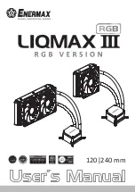
ELC-LMT120-RGB
Бренд: ENERMAX Страницы: 33

RAID 6
Бренд: InfoStor Страницы: 6

HZA-PWR-15A
Бренд: Crestron Страницы: 2

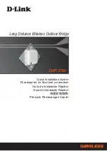
DAP-3711
Бренд: D-Link Страницы: 54

DCS-2210
Бренд: D-Link Страницы: 67

DAP-2590 - AirPremier N Dual Band PoE Access Point
Бренд: D-Link Страницы: 44
DAS-3 Series
Бренд: D-Link Страницы: 14

DAP-3520 - AirPremier N Dual Band Exterior PoE Access Point
Бренд: D-Link Страницы: 80
DAP-3760
Бренд: D-Link Страницы: 128


