background image


DIGITAL 


 In the interests of user-safety the set should be restored to its

original condition and only parts identical to those specified be
used.

Page

SAFETY PRECAUTION FOR SERVICE MANUAL ...........................................................................................................

2

VOLTAGE SELECTION .....................................................................................................................................................

2

AC POWER SUPPLY CORD AND AC PLUG ADAPTOR .................................................................................................

3

SPECIFICATIONS .......... . .................................................................................................................................................

3

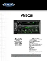
NAMES OF PARTS ...........................................................................................................................................................

4

OPERATION MANUAL.. ......

... .. ...................................................................................................................................

6

DISASSEMBLY.. ................... .............................................................................................................................................
REMOVING AND REINSTALLING THE MAIN PARTS.. .................................................................................................
ADJUSTMENT .................................................................................................................................................................

13

BLOCK DIAGRAM ...........................................................................................................................................................

17

SCHEMATIC DIAGRAM/WIRING SIDE OF 

...........................................................................................

VOLTAGE ............ ............................................................................................................................................................

38

NOTES ON SCHEMATIC DIAGRAM ..............................................................................................................................
TYPES OF TRANSISTOR AND LED.. ..............................................................................................................................

39

WAVEFORMS OF CD CIRCUIT.. ....................................................................................................................................

40

. .................................................................................................................................................

41

FUNCTION TABLE OF

.................................................................

............................................................................

45

FL DISPLAY.. ....................................................................................................................................................................

53

REPLACEMENT PARTS LIST/EXPLODED VIEW


This document has been published to be used
for after sales service only.
The contents are subject to change without notice.

Summary of Contents for CD-M4000

Page 1: ...WER SUPPLY CORD AND AC PLUG ADAPTOR 3 SPECIFICATIONS 3 NAMES OF PARTS 4 OPERATION MANUAL AL 6 DISASSEMBLY REMOVING AND REINSTALLING THE MAIN PARTS 1 ADJUSTMENT 13 BLOCK DIAGRAM 17 SCHEMATIC DIAGRAM WIRING SIDE OF P W BOARD 20 VOLTAGE 38 NOTES ON SCHEMATIC DIAGRAM 39 TYPES OF TRANSISTOR AND LED 39 WAVEFORMS OF CD CIRCUIT 40 TROUBLESHOOTING 41 FUNCTION TABLE OF IC 45 FL DISPLAY 53 REPLACEMENT PARTS ...

Page 2: ... REPLACEMENT SERVICE PARTS ARE ALL FACTORY PRESET BEFORE SHIPMENT DO NOT ATTEMPT TO READJUST THE LASER PICKUP UNIT DURING REPLACEMENT OR SERVICING 3 UNDER NO CIRCUMSTANCES STARE INTO THE PICKUP LENS AT ANY TIME 4 CAUTION USE OF CONTROLS OR ADJUSTMENTS OR PERFORMANCE OF PROCEDURES OTHER THAN THOSE SPECIFIED HEREIN MAY RESULT IN HAZARDOUS RADIATION EXPOSURE CLASS 1 LASER PRODUCT APPAREIL i LASER DE ...

Page 3: ...kohms n CD player n Tuner Frequency range FM 88 108 MHz AM 531 1 602 kHz w Cassette deck Frequency response 50 14 000 Hz Normal tape Signal noise ratio 55 dB TAPE 1 Dlavbackl 150 dB TAPE 2 din playback Wow and flutter IO 3 IWRMS1 TYPO 4 way type speaker system Super Tweeter 8 cm 3 118 Tweeter 8 cm 3 118 Midrange 25 cm lo Woofer Maximum input power 300 W Total Rated input power 150w Total Impedance...

Page 4: ...rd Play Button with Indicator 24 Tape 2 Reverse Mode Select Button 25 CD Track Up or Fast Forward Tape 2 Fast Wind Tuner Preset Up Button 26 Tuning and Time Down Button 27 Memory Set Button 28 Tape 2 Record Pause Button 29 CD Track Down or Fast Reverse Tape 2 Fast Wind Tuner Preset Down Button 30 Microphone Level Control 31 Microphone Socket n Display 1 FM Stereo Mode Indicator 2 FM Stereo Receivi...

Page 5: ... Preset Down Button 8 Equalizer Mode Select Button 9 Tape 2 Reverse Play Button lO CD Button 11 Tuner Band Button 12 0n Stand by Button 13 Monster Bass Button A 2 3 4 14 Q 15 A5 16 is 6 17 18 7 19 8 20 9 IO 21 11 22 12 14 CD Random Button 15 CD Memory Button 16 CD Pause Button 17 CD Track Up or Fast Forward Tape 2 Fast Wind Tuner Preset Up Button 18 CD or Tape Stop Button 19 CD Play or Repeat Tape...

Page 6: ...it using the AC plug adaptor supplled with the urxt as illustrated The AC plug adaptor IS not included in areas where the wall socket and AC power plug can be directly connected see lllustratlon 0 n Setting the FM AM span selector The International TelecommuntcatlonUnion ITU has establlshed that member coun trues should maintain either a 100 kHz or a 50 kHz interval between broadcastingfre quencle...

Page 7: ...button once to advance the time by 1 minute Hold it down to change the bme in 5mmute Intervats s The hour will not advance even if minutes advance from 59 to 00 I l The clock begins counting from 0 seconds Seconds are not displayed The time dlsptay will disappear after a few seconds To confirm the time display Press the CLOCK button The time display will appear for about 5 seconds Note The CLOCK o...

Page 8: ...lead of the unit plugged stopped in the middle of a track l e discverydIm Is the battery olarfty respected Has condensation formed inside the unit Is the distance or angle incorrect w Tuner Does the rem control sensor recewe l Radio makes unusual noise con Is the unit placed near the TV or comput Is the FM aerial or AM loop aerial placed properly Move the AC power lead away from the aerial if loca...

Page 9: ... 1 o 4 2 Screw Ji x5 1 Screw Kl xl lo 4 1 Screw Ll x2 10 4 1 Hook Ml x2 10 5 2 Cover M2 xl 1 Turn fully the lock lever in the 9 3 arrow direction 2 Whileholdingthelocklever rotate 1 O l the cam gear until the cam gear rib engages with the clamp lever 3 Push the slide chassis backward to 1 O 6 engage the claw with the groove and remove it in the direction of the arrow Nl x6 1 Screw Pi xl 11 1 2 Hoo...

Page 10: ...CD M4000W CP M4000 Clamp Lever CD Player Unit Top View Cam Gear Rib Figure 10 l E3 x1 y b Figure 1 O 2 Push iPush 1 Figure 1 O 3 w Figure 1 O 4 urntable Figure 10 5 Nl x 3 Figure 10 6 ...

Page 11: ...Holder A2 x4 3 Woofer 1 Screw Cl x4 1 l 5 4 Tweeter 1 Screw Dl x4 11 5 5 Midrange 1 Screw El x4 11 5 Mechanism Figure 11 2 Front Panel moxAss 3 Screw A3 x4 2 Super Tweeter 1 Screw Bl x2 11 5 Figure 11 4 Figure 11 3 Sneaker Box Ass y Figure l l 5 ll ...

Page 12: ... Carefully bend the pinch roller paw1 in the direction of the arrow AZ and remove the pinch roller Cl x 1 PC in the direction of the arrow cB Note When installing the pinch roller pay attention to the spring mounting position How to remove the belt TAPE 2 See Fig 12 4 1 Remove the main belt Dl x 1 PC from the motor side 2 Remove the FF REW belt D2 x 1 pc How to remove the belt TAPE 1 See Fig 12 4 ...

Page 13: ... removing the connector for the optical pickup from the connector wrap the conductive aluminium foil around the front end of connector so as to protect the optical pickup from electrostatic damage CD M4000W CP M4000 CD Loading Motor Figure 13 1 B4 x 1 Gear B2 x 1 Figure 13 2 ADJUSTMENT MECHANISM SECTION l Tape Speed l Driving Force Check Torque Meter Play TW 2111 Specified Value Tape 1 Over 80 g T...

Page 14: ...are performed automatically Therefore playback of each disc can be performed under optimum conditions Items adjusted automatically 1 Offset adjustment The offset voltage between the head amplifier output and the VREF reference voltage is compensated inside the IC Focus offset adjustment Tracking offset adjustment 2 Tracking balance adjustment waveform drawing Fig 14 2 EFBL 3 Gain adjustment The ga...

Page 15: ...each 2 set a FOF XXXX b TOF XXXX c TBA XXXX d TGA XXXX f FGA XxXx g RFL XXXX 177 key Track 4 2 7 key Track 9 3 key Track 15 explanation a Focus off set FOF XXXX I b Tracking off set TOF XXXX c Tracking balance TBA XXXX d Tracking Gain TGA XXXX f Focus Gain FGA XXXX g RF level shift RFL XXXX VOL Last memory BAL CENTER P GEQ FLAT X BASS OFF To cancel Power OFF I Laser ON MEMORY key input Tracking OF...

Page 16: ...rror ER CD Tray Error ER CD Micon Communication Error ER CD Focus Not Match NO DISC IL Time Over NOT READ TUN PLL Unlock ER TU Notes 00 While in Protect Circuit Operate 01 Over Current Detection 02 DC Detection 03 00 Tape Mechanism Error 01 Initial Error 02 03 00 Pickup Mechanism Error 01 PU IN SW Detection NG 02 03 10 Changer Error 11 Initial Error 12 13 20 Tray Error 21 22 23 30 System VCD 31 Sy...

Page 17: ...CD M4000W CP M4000 TO DISPLAY SECTION c 61 CE 62 CL 63 DI 64 DO 65 wmo 6 VRES 6 DRF ICI LC78645E CD SERVO CONSTANT VOLTAGE SW4 PICKUF IN Figure 17 BLOCK DIAGRAM i 3 17 ...

Page 18: ...TENNA vr x352 I I I rm 4 5MHZ JKl ICKl I I I I M65656SP MIC AMP B4 f JK601 VIDEO AUX IC601 P 7CO CNSll KIR FROM CD SERVOSIS TION WI L CH es F BACK R CH SWITCt REC MOTOR DRIVER BIAS Figure 18 BLOCK DIAGRAM 2 3 18 ...

Page 19: ...I I _ _ _ SYSTEM MICROCOMPUTER El 1 I B5 4 1943 MHz SP DET 1 Q901 Q9iq 2OdB ATT IC B 7 605 606 g SP RELAY ON OFF 1 so901 SPEAKER TERMINAL T601 POWER TRANSFORMER RECIPLAY F607 T2A L 250V I A SW801 VOLTAGE SELECTOR VFl TliJ2 VF AC POWER SUPPLY CORD AC 1 I Oil 27 220 230 240 V 50 60 Hz BIAS Figure 19 BLOCK DIAGRAM 3 3 19 ...

Page 20: ... 2 d Y 1 2 i J 3 _ L 4 5 I 11 1 6 7 6 t Cl L I I I III E 1111 I I PUIN GND I Y NP3 F I Fk L w I I I L G I CD SIGNAL E VCC I VREF 1 E 1 EC LASER DRIVER I H l NOTES ON SCHEMATIC DIAGRAM can be found on page 39 1 2 3 j 4 1 5 6 J Figure 20 SCHEMATIC DIAGRAM l 10 2o ...

Page 21: ...SLRCK 1 GMOUT EFLG c51 I 0 022 T 1 R CH AGND 8 L CH _ c DGND y 5v _ 5 I 5v _ 6 II C42 3 01 r I CNP _ 2TtNi E ICl C78645E f53trwu hrrs Ih C48 D 022 I m KTC 03 Y l The numbers to are waveform numbers shown in page 40 7 8 9 10 Figure 21 SCHEMATIC DIAGRAM IO 2l 11 12 I ...

Page 22: ...CDrM4000W CP M4000 IC601 LC75341 AUDIO PROCESSOR r l NOTES ON SCHEMATIC DIAGRAM can be found on page 39 Figure 22 SCHEMATIC DIAGRAM 3 l 0 22 ...

Page 23: ...CD M4000W CP M4000 __ __ _ _ _ __ _ _ I FM SIGNAL MAIN PWB l z w PLAYBACK SIGNAL RECORD SIGNAL N CD SIGNAL DD VIDEO SIGNAL _ _ _ _ _ _ I CNPGD1 1 7 8 9 10 Figure 23 SCHEMATIC DIAGRAM 4 l 0 23 11 12 I ...

Page 24: ...CDiM4000W CP M4000 NSPLAY PWB Bl A B C D E F G H MICRC IC704 KIA4558P OPE AMP l NOTES ON SCHEMATIC DIAGRAM can be found on page 39 1 2 3 4 5 6 1 Figure 24 SCHEMATIC DIAGRAM 5 l 0 24 ...

Page 25: ...CD M4000W CP M4000 3 R7W K INPUTiOUTPUTEXPANDER I I I I I i i i i i 7 8 9 10 Figure 25 SCHEMATIC DIAGRAM 6 l 0 25 11 12 I ...

Page 26: ...CD M4000W CP M4000 _ __ __ __ __ P F_ POWER AMP I POWER PWB Di Ad I_ _ _ _ l NOTES ON SCHEMATIC DIAGRAM can be found on page 39 1 I 2 I 3 I 4 I 5 I 6 I Figure 26 SCHEMATIC DIAGRAM 7 10 26 ...

Page 27: ...CD M4000W CP M4000 FM _ ____ SIGNAL R CH 1 wJ SC m SPEAKER GND TERMINAL I I CS I J I I _ 1 _ ___ I 7 a 9 10 11 12 I Figure 27 SCHEMATIC DIAGRAM 8 10 27 ...

Page 28: ... r _ _ c314 0 0047 D305 DS1SSW I c315 0 0047 FM FRONT END 22P R309 CF303 WI iOK FM SIGNAL R316 fS AM SIGNAL 47K I e I s IC302 LC72131 PLL TUNER IC303 LA1 8328 FM IF DET FM MPX AM IF I l NOTES ON SCHEMATIC DIAGRAM can be found on page 39 1 2 3 4 5 I 6 J Figure 28 SCHEMATIC DIAGRAM 9 l 0 28 ...

Page 29: ... M4000W CP M4000 MIC PW H bD MIC SIGNAL I I l NOTES ON SCHEMATIC DIAGRAM can be found on page 39 Figure 29 SCHEMATIC DIAGRAM IO lo MAIN PWB P30 6 A 7 a 9 11 12 Figure I 29 WIRING SIDE OF P dmLOARD l 9 29 ...

Page 30: ... 3 4 5 6 7 8 9 1 0 I I I T 3o3fl3 a3fl A B C D E F G H L r FM 75 OHM so301 FM ANTENNA TERMINAL L GND AM LOOP ANTENNA SPAN SELECTOR 9 kHdfi0 kHz r 2 L 10 kHd 100 kHz l R606 g R613e3 e i 1 L 1 1 2 3 4 I 5 6 Figure 30 WIRING SIDE OF P W BOARD 2 9 30 ...

Page 31: ...14Om jtC124 R142B ii C136 s j t 3 mR126 102 CNS102 R124 lcllt m ___ ___ EERlO5 EElR o6 II c154 1 IP37 11 F TA 2 RECORD PLAYBACK ERASE HEAD I P37 10 F FROM TAPE 1 PLAYBACK HEAD 607 f l k C621 cd59 ii C609 w R653 C625 i t C852 C629 l I R624 R852 TO AMP PWB P35 12 E a 9 10 11 12 I Figure 31 WIRING SIDE OF P W BOARD 3 9 31 ...

Page 32: ...CNS CNS DISPLAY PWB Bl P34 3 G S7025 tflcs713 J CNP702 r 2 q 702 I J q MONSTER BASS PWB B3 TO TAPE MEC SM i31k f Bl704 _ _ _ 1 2 3 4 5 I 6 Figure 32 WIRING SIDE OF P W BOARD 4 9 32 ...

Page 33: ...r i I I _ 1 D36f3 I I L J JTAPE I I I I C 1 _ I 1 18 SW7114 Dl3B L J L d RI 7111 AL 1 a L DIMME 1R LED702 RL70rn 5 15 I I n r i LCUC 1n m705 3 E LED705 I r 7 SW732 IC702 I I N716 U LIZER E I _ I I E g L J I s 1 r 7 r 1 J _ I _ I W 8 1 s _ 3 I I I t RDOl J RLi06 L J RD32 RD3 m L J SW730 RD02 EEj RL707 j RD3O m B r 7 I I RL708 1 RD29 EERSE _ 1 I _ I gg7 r 7 ii I L FORWARD f a T l SW726 I s FAST 1 l ...

Page 34: ...L i VIOLET 1 TRANSFORMER PWB D3 1 I AC POWER SUPPLY CORD f AC I 1 Oil 27 220 230 240 V 50160 Hz I T801 POWER TRANSFORMER HEADPHONES PWB B2 I I I I 1 JK670 HEADPHONES fk5 J i c q 1 I 1 2 3 4 5 6 Figure 34 WIRING SIDE OF P W BOARD 6 g 34 ...

Page 35: ...CP M4000 MD01 BR FAN MOTOR CNS904 CNS903 Jt Cf I 0908 1 i T I I T I 8 I_ Bl903 i I I i 7 i I R949 D913 I C946 Fl950 c952 w I R943e I 1234 CNS902 mw P3 7 H 7 8 9 10 Figure 35 WIRING SIDE OF P W BOARD 7 9 35 11 12 ...

Page 36: ...VO PWB C P32 1 B FROM DISPLAY PWB P30 4 A FROM MAIN PWB CNSlA CNSll CNS2A CNS PICKUP UNIT 306 j l The numbers to are waveform numbers shown in page 40 CNSBA CNSBB 1 I 2 I 3 4 I 5 I 6 J Figure 36 WIRING SIDE OF P W BOARD 8 9 36 ...

Page 37: ...E MECHANISM PWB F SOLENOID A M3 jTAPdlJ PLAYBACK HEAD P31 12 F TO MAIN PWB CD LOADING MOTOR PWB E SOLENOID ITAPE2 RECORDIPLAYBACWERASE HEAD P31 12 D FROM MAIN PWB 7 a 9 10 11 I 12 I Figure 37 WIRING SIDE OF P W BOARD 9 9 37 ...

Page 38: ...CD iVi4000W CP M4000 VOLTAGE 38 ...

Page 39: ... prior notice 9 The indicated voltage in each section is the one measured by Digital Multimeter between such a section and the chas sis with no signal given 1 In the tuner section indicates AM indicates FM stereo 2 In the main section a tape is being played back 3 In the deck section a tape is being played back indicates the record state 4 In the power section a tape is being played back 5 In the ...

Page 40: ...CD M4000W CP M4000 WAVEFORMS OF CD CIRCUIT IIII l l I DRF Q ICl Q Cl Q ICI Q lCl Q Cl ICl I Cl ICl CH4 cum Hold on 0 2 ps 40 ...

Page 41: ... has the mark next to it 2 Place the CD cleaner disc onto the CD disc tray with the brush side down then press the play button Cleaning fluid 3 You will hear music for about 20 seconds and the CD player will automatically stop If it continuous to turn press the stop button l The CD lens cleaner should be effective for 30 50 operations however if the brushes become worn out earlier then please the ...

Page 42: ...eck the focus peripheral circuit I I No 3 Is the laser lit Check the laser diode driver Cl peripheral circuit 4 Is the turntable rotating When a disc is loaded start playback operation No Spindle motor Ml 1 Is focus servo activated Waveform drawing Figure 42 2 No Pins 7 12 79 and 80 on ICl Check the laser diode driver Cl peripheral circuit I Yes No Is the disc rotating No Check the spin system I I...

Page 43: ... cannot be completed or the beginning of the track cannot be found No Check the around pin 20 on ICl v Initialization is not possible I Data cannot be read Check the VCO PLL system Figure 43 1 Press the OPEN CLOSE switch without inserting a disc and then try starting the play operation 1 The turntable rotates a little Waveform drawing The spin driver circuit is OK Figure 43 2 Yes No 2 The turntabl...

Page 44: ...W CH4 0 W Figure 44 1 The HF waveform is normal and the time is displayed normally but no sound is produced Or the sound has dropouts No There are too many error flags on a damaged disc which makes error correction impossible 1 When playing at normal speed Check the peripheral circuit at pin 39 DOUT on ICl and the waveform Figure 44 2 1 Check again using a known good disc If OK Check the unit 1 44...

Page 45: ...t used set them as input terminals and connect SBCWCONTG Input Output Input Mode General purpose I O terminal 6 or to 0 V or set them as output Subcode reading clock input terminal terminals and leave open I SBCK FG Subcode reading clock input terminal FG signal input terminal external j not used connect to O V emphasessetting termrnal Terminal functions are set by commands When 29 1 DEFECT 1 outp...

Page 46: ...n this unit the terminal with asterisk mark is open terminal which is not connected to the outside Be sure to supply the same potential to each power terminal VVDD ADAVDD VDD LVDD RVDD XVDD Terminal witch is controlled by the power terminal VDD5V for a microcomputer interface CE 61 pin CL 62 pin Di 63 pin DO 64 pin WRQ 65 pin RES 66 pin DRF 67 pin 46 ...

Page 47: ...1 CD Servo LC78645E E 2 8 F58Ed8 60 79 78 77 76 75 74 73 72 a DATA 3 DATACK EFMIN 3 z LRSY RF RFVDD RFVSS FIN1 FIN2 TIN1 TIN2 VREF REFI FE TEC TE RFMON JITTC ADAVDD ADAVSS TDO LC78645E CORRECTION A DlO CD Figure 47 BLOCK DIAGRAM OF IC 47 ...

Page 48: ... input 1 kHz AN13 SPEANA 0 Input Speana data input 63 kHz ANl2 AN10 KEY P KEY 0 Input Key input AVDD AVDD Input Analog VDD AVREF AVREF lnout Analoa REF voltaae 36 1 lNTP3 1 P IN I lnout 1 Power failure detect I 37 PO2 JOG 1 Input JOG volume input 1 38 PO1 JOG 0 Input JOG volume input 0 39 INTPO REMOCON Input Remocon input 40 v s s v s s Ground voltage 41 P74 SMUTE output System mute control 42 P73...

Page 49: ...2 DIST2 Input Destination input FIP31 P21 output FL display driver PlOl DlSTl Input Destination input FIP30 P20 output FL display driver Pl 00 DISTO lnout Destination input I FIP29 I Pl9 I Output I FL displav driver I 71 78 I FIP28 FIP21 Pl8 PI1 I Output I FL displav driver I 79 VLOAD VLOAD Input FL driver power supp 30 V 80 89 j FIP20 FIPll 1 PlO PI I Output I FL display driver I gO 100 1 FIPlO F...

Page 50: ...CD M4000W CP M4000 IC6pl VHiLC75341bl Audio Processor LC75341 i E LOUT 4 LBASS 5 0 1 UF LTRE LIN h l F I 1 ROUT g RBASS O luF g RTRE g RlN 3 RSELO ...

Page 51: ...gital delay 16 LPFl IN2 Input Low pass filter 1 input 2 Pre filter before A D convertor for digital delay 17 LPFI O U T output Low pass filter 1 output Pre filter before A D convertor for digital delay 18 AD INTOUT output A D integrator output Composes D A conversion integrator with external capacitor 19 AD INTIN Input A D integrator input Composes D A conversion integrator with external capacitor...

Page 52: ...g output 36 L OUT output Lch mixing output 37 VCF IL Vocal cut filter Processes frequencies lower then the vocal band 38 PSI Input Phase shift input 1 Determines a constant at time of phase shift 39 PS2 Input Phase shift input 2 Determines a constant at time of phase shift 40 LATCH Input Latch input via serial bus 41 CLOCK input Clock input via serial bus 42 DATA input Data input via serial bus In...

Page 53: ...CD M4000W CP M4000 FL DISPLAY FL701 VVKBJll LM02Ti FL Display 11G IOG 6 Sl Si Sl gf d q ...

Page 54: ...ced stored in a retrieval system or transmitted in any form or by any means electronic mechanical photocopying recording or otherwise without prior written permission of the publisher SHARP CORPORATION AV Systems Group Audio Systems Division Higashihiroshima Hiroshima 739 0192 Jaw Printed in Japa L A01 09 l 463DSeHAeM SA St EX ...

Reviews: