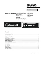
background image


Service Manual 

Full Panel Detachable 
High Power 
FM/AM Stereo 
Receiver 
Compact Disc Player


FXD-680GD 

114782877 

FXD-685GD 

114782878


SEL

FM/MW/LW CD RECEIVER    45W x 4    CD-R&RW

FXD-680GD

SEL

FM/MW/LW CD RECEIVER    45W x 4    CD-R&RW

FXD-685GD


Contents 


SERVICE NOTE AND PRECATIONS............................................................................................................................................................................... 2 

OPERATION CHECK ....................................................................................................................................................................................................... 5 

ALIGNMENT LOCATIONS................................................................................................................................................................................................ 6 

ELECTRICAL ADJUSTMENTS......................................................................................................................................................................................... 7 

BLOCK DIAGRAM .......................................................................................................................................................................................................... 18 

IC/TRANSISTOR LEAD IDENTIFICATION..................................................................................................................................................................... 20 

CD MECHANISM EXPLODED VIEW ............................................................................................................................................................................. 21 

CABINET & CHASSIS EXPLODED VIEW ...................................................................................................................................................................... 22 

PART LIST – CD MECHANISM ...................................................................................................................................................................................... 23 

PART LIST CABINET, CHASS AND ACCESSORY ....................................................................................................................................................... 25 

PART LIST MAIN ............................................................................................................................................................................................................ 27 

PART LIST KEY.............................................................................................................................................................................................................. 30 

PART LIST CD SERVO .................................................................................................................................................................................................. 31 

PART LIST REMOTE...................................................................................................................................................................................................... 33 

PART LIST JB/GIB.......................................................................................................................................................................................................... 34 

SCHEMATIC DIAGRAM ................................................................................................................................................................................................. 35 

CIRCUIT BOARD DIAGRAM .......................................................................................................................................................................................... 39


REFERENCE No. SM-06

0

00

03


FILE NO

Summary of Contents for FXD-680GD

Page 1: ...CE NOTE AND PRECATIONS 2 OPERATION CHECK 5 ALIGNMENT LOCATIONS 6 ELECTRICAL ADJUSTMENTS 7 BLOCK DIAGRAM 18 IC TRANSISTOR LEAD IDENTIFICATION 20 CD MECHANISM EXPLODED VIEW 21 CABINET CHASSIS EXPLODED VIEW 22 PART LIST CD MECHANISM 23 PART LIST CABINET CHASS AND ACCESSORY 25 PART LIST MAIN 27 PART LIST KEY 30 PART LIST CD SERVO 31 PART LIST REMOTE 33 PART LIST JB GIB 34 SCHEMATIC DIAGRAM 35 CIRCUIT ...

Page 2: ...tivity MW 32 dBµ S N 20 dB Signal to Noise Radio More than 45 dB LW TUNER Frequency Range LW 144 288 kHz Sensitivity LW 35 dBµ S N 20 dB CD PLAYER Frequency Response 20Hz 20 000Hz Signal to Noise Radio More than 65 dB Channel Separation More than 60 dB T H D Less than 0 30 AUDIO AMPLIFIER GENERAL Output Power 4 X 45 W Speaker Output Impedance 4 ohm Power Source DC 12V Negative ground Specification...

Page 3: ... 5 Non metallic alignment tools must be used especially at FM alignment 6 for alignment location details refer to CIRCUIT BOARD PARTS LOCATIONS Installation procedure 1 To prevent a short circuit remove the key from the ignition and disconnect the battery 2 Make the proper input and output wire connections for each unit 3 Connect the wiring harness wires in the following order ground sealers batte...

Page 4: ...ircuit board 3 Each and every pickup is already individually adjusted to a high degree of precision and for that reason the adjust ment point and installation screws should be absolutely never be touched 4 Laser beam may damage the eyes Absolutely never permit laser beams to enter the eyes Also NEVER switch ON the power to the laser output part lens etc of the pickup if it is damaged Laser Beam NE...

Page 5: ...make a short circuit in the area indicated in Fig 2 first Then remove the pickup and perform the work 3 The CD pickup OPTIMA 725C2 which is supplied as one of the spare parts is already short circuited with the copper foil pattern pre soldered indicated in Fig 2 below To handle this CD pickup keep the short circuit as it is Then attach the pickup to the unit and connect the flexible wire to the co...

Page 6: ...tput level FM MW LW Power source voltage DC 14 0V Backup voltage is the same as this AF load impedance 4 ohm pure resistance Balance Center position of level Tone Center position The signal strength read in this section is voltage on the antenna Test Diagram FL SPK FR SPE BACK UP 14 4V GROUND POWER ANTANNA MPX STEREOS MODULATOR FM SG AM SG DUMMY ANTANNA VTVM VTVM DISTORTION METER ACC DV14 4V SPK R...

Page 7: ...6 ALIGNMENT LOCATIONS FM TUNER ...

Page 8: ...ep Generator Coupling Generator Display Setting Adjustment Remarks Stereo Separation Signal Generator to antenna receptacle 98 1 MHz Int 1 kHz Dev 75 kHz L R 90 pilot 10 98 1 MHz VR1 Adjust AF output power at maximum separating more than 30 dB FM SNC Adjustment 98 1 MHz Dev 75 kHz L R 90 Int 1 kHz 60dBµV output 98 1 MHz 40 dBµ 98 1 MHz VR2 Stereo Separation 25 dB 5 dB STOP SENS Signal Generator to...

Page 9: ...MANUAL appears on the display the manual tuning mode is selected If both buttons have not pressed for several seconds it will revert to seek tuning mode and AUTO appeared on the display AUTOMATIC MEMORY STORING PROGRAM SCANNING 4 Automatic memory storing Press P SCAN AST button 4 for several seconds the radio searches for 6 strongest stations and stores them into the presets of the currently selec...

Page 10: ...ocal or distant stations Use local position LOCAL LOC appears on the display for reception of strong station and distant position DX appears on the display for reception of weaker stations This function is effective during AUTO SEEK operation MONO STEREO SELECTION 7 Press MONO button 7 to select mono or stereo mode You can sometimes improve reception of distant stations by selecting mono operation...

Page 11: ...s played the unit returns to the first track and play resumes SKIPPING TRACKS 3 Press the TUN TRK button to skip to the beginning of the next track Press the TUN TRK button to skip to the beginning of the previous track Press and hold the TUN TRK or TUN TRK button 3 for several seconds to search quickly with sound in the forward or reverse direction When the button is released the CD resumes norma...

Page 12: ...o begin shuffle play To cancel this mode press the SHF button 7 again SCAN MODE PLAYING THE BEGINNING OF EACH TRACK 5 This function plays the first several seconds of each track sequentially Press the SCN button 5 to begin the scan mode To cancel this mode press the SCN button 5 again During playback of a CD the CD running indicator spins The unit will turn on automatically when a CD is inserted i...

Page 13: ...WITCHING TO AUX MODE 1 The unit has a pair of auxiliary input terminals see WIRING figure on page 18 This allows you to listen to an auxiliary audio source MP3 portable cassette player etc Press the SOURCE button 1 with the power on to switch from radio mode or CD mode to AUX mode ...

Page 14: ...aying a CD press the PAU button 3 To resume playing press the PAU button 3 again SCAN MODE PLAYING THE BEGINNING OF TRACKS OR DISCS 4 This function plays the first several seconds of each track or disc sequentially Playing the beginning of tracks Track Scan Press the SCN button 4 to play the first several seconds of each track on the current disc in order Playing the beginning of disc Disc Scan Pr...

Page 15: ... SHF button 6 for several seconds The system selects a disc at random and plays all tracks on that disc When all tracks have been played the next disc is selected and Shuffle playing is repeated To cancel the track shuffle or disc shuffle mode press the SHF button 6 again SELECTING A DISC 7 8 Press the DISC button 7 to select the preceding disc Press the DISC button 8 to select the next disc Note ...

Page 16: ... FXD 680GD FXD 685GD POWER VOL TUN TRK VOL LOUD AST PAU SCN RPT SHF 1 5 3 6 4 9 10 15 13 2 7 8 11 14 12 1 POWER 2 AUDIO 3 VOL 4 VOL 5 SOURCE 6 TUN TRK 7 TUN TRK 9 BAND LOUD 10 PAU 11 SCN 12 RPT 13 SHF 14 SOUND 15 1 6 Preset buttons ...

Page 17: ...or the player If this occurs wait for the road surface to improve before using the CD player Safety For safer driving keep the volume at a moderate level to enable you to hear outside sounds such as emergency vehicle sirens Cleaning the unit Clean the unit with a soft dry cloth Stains should be removed by wiping the surfaces with a soft cloth immersed in lukewarm water and wrung dry Never use stro...

Page 18: ...17 ELECTRICAL ADJUSTMENTS DUMMY BOX SCHEMATIC AM DUMMY ANTENNA FM DUMMY ANTENNA ...

Page 19: ...18 BLOCK DIAGRAM FOR FXD 680GD ...

Page 20: ...19 BLOCK DIAGRAM FOR FXD 685GD ...

Page 21: ...20 IC TRANSISTOR LEAD IDENTIFICATION ...

Page 22: ...21 CD MECHANISM EXPLODED VIEW MECHANSIM 94 01683 10 ...

Page 23: ...22 CABINET CHASSIS EXPLODED VIEW ...

Page 24: ...0 03 9 RPPOM F20 03 10 RPPOM F20 03 11 RPPOM F20 03 12 RPPOM F20 03 13 RPPOM F20 03 14 RPPOM F20 03 15 RPSUM24L NI 4 RPSECC T1 0 1 RPFF 050SH 11190 RPPOM F20 03 16 RPGLASS EPOXY RPP H TTS 2 2 RPSUS304WPB 3 RPPOM F20 03 17 RPSUS304WPB 4 RPSEEC T1 0 2 SENSOR SENSOR PCB SCREW COVER UPPER LEVER DISC GUIDE UP BUSHING ROLLER ROLLER DISC SHAFT ROLLER PIN ROLLER PVC CAP B K ROLLER PIN PULLEY PIN IDLE GEAR...

Page 25: ...M S 2 2 RPFF 050SH 11190 RPPOM F20 03 21 RPKNN11 PCD18 RPR H W W TTB2 5 RP1007 28 RPSUS304WPB 7 RPPOM F20 03 22 RPBSBM RPSW 110 RPB H TTB1 7 8 RPSF C99 RPPOLY AMIDE RPRUS T0 2 RP RP0 55 RP4 5 18 RPPE 2 RPSW 111 RPPE 3 RPSUS304WPB 8 CLAMP DISC HOLD CLAMPER S P CLAMPER TURN TABLE BASE PU PIN SIDE A SCREW PIN SIDE B DAMPER S P BASE MOTOR GEAR PU B GEAR PU A SCREW MOTOR HOUSING GEAR SHAFT PU SCREW 4P ...

Page 26: ...RP40 05018 04 RP52 V3651 00 RP40 02604 01 RP40 02606 01 RP40 02608 01 RP40 02610 01 RP40 120080 21 RP40 12606 01 Panel Trim Ring S OPC1202 Base For CD CD MECHA CDM 1683 EUR 143A W O PCB Main Bracket CD Bottom Cover Main Fiber Main Board Mounting Box Shade II PC Plate CD Hook Plate FIX Bracket For Slide Lock Plate Spring Locked 0 35 Shaft Locker Spring Ø0 70 Lock Spring Heat Sink 4 IC Bracket Socke...

Page 27: ...cription RP35 40005 00 RP35 50001 00 RP39 00128 00 RP40 05006 07 RP40 15025 11 RP39 V3610 00 RP51 A8026 00 HEXAGON NUT M5 SPRING WASHER M5 METAL BAR 197MM SCREW Ø5X6 RH MS SCREW Ø5X25 TA ST KEY 1 0 CARYING CASE Mounting Strap Locking Screw Unlock Levers Carrying Case ...

Page 28: ...3 00A RP05 05220 00A RP05 05223 00A RP05 05272 00A RP05 05330 00A RP05 05332 00A RP05 05562 10A RP05 63101 00 RP05 63102 01 RP05 63104 01 RP05 63153 01 RP05 63223 01 RP06 00473 11 RP06 10107 02E TR BD435 NPN TO 126 SAMSUNG TRANSISTOR 2SA1175 FF TRANSISTOR B1240 TRANSISTOR 2SC2785 NEC TRANSISTOR 3792C IC REGULATOR 78L05 TR 8050C TO 92 B DIODE IN4001 TAPPING DIODE 1N4148 72 ROHM DIODE 1 5KE 30A ZENE...

Page 29: ...07 05124 54 RP07 05153 16A RP07 05220 16A RP07 05221 16A RP07 05222 16A RP07 05223 16A RP07 05224 54 RP07 05272 16A RP07 05330 16A RP07 05331 16A RP07 05332 16A RP07 05333 16A RP07 05334 16A RP07 05393 16A RP07 05471 16A E CAP 220µF 10V Ø8X5MM 105 C E CAP 47µF 10V Ø5X7MM MINI E CAP 10µF 16V Ø6 3X5MM E CAP 10µF 16V Ø4X5MM RC3 E CAP 100µF 16V Ø8X5 ELNA E CAP 22µF 16V Ø5X5 ELNA E CAP 3300µF 16V 105 C...

Page 30: ...7021 025 RP12 12068 411 RP15 00003 05 RP16 00244 00 RP25 08370 16 RP25 17020 02 RP25 17020 04 RP25 17068 36D RP25 M1702 50 RP25 M1702 80 RP29 00347 02 RES 4 7kΩ 1 16W TAPPING RES 47kΩ 1 16W TAPPING RES 470kΩ 1 16W TAPPING RES 5 6kΩ 1 16W TAPPING RES 68Ω 1 16W TAPPING RES 680Ω 1 16W TAPPING RES 6 8kΩ 1 16W TAPPING RES 75Ω 1 4W RES 8 2kΩ 1 16W TAPPING RES 82kΩ 1 16W TAPPING CHIP RES 1kΩ 5 0603 SMT C...

Page 31: ...1 17020 305 RP16 01107 02K RP18 00163 00 RP25 M1475 00 RP27 17020 00 E S D DIODE NNCD6 2G 5PIN SMD LED FR1112H RED STANLEY FA1112H ORANGE SMD LED STANLEY CD1702 LCD B L 97X17 AMBER IC LC75823ED CHIP 0 1µF 10 X7R 0603 SMT CHIP 680PF 5 NPO 0603 SMT CHIP RES 0Ω 0603 SMT CHIP RES 10Ω 5 0603 SMT CHIP RES 1kΩ 5 0603 SMT CHIP RES 1 5kΩ 5 0603 SMT CHIP RES 180Ω 5 0603 SMT CHIP RES 1 8kΩ 5 0603 SMT CHIP RE...

Page 32: ...4 00 RP07 63105 00 RP07 63124 00 RP07 63153 00 TR KRC103S NPN SOT 23 KEC TR 2SA812 PNP TO 92M NEC RANSISTOR 2SD1225M NPN ATV ROHM IR LED MIE 144A1MC ZENER DIODE 3 6V 0 5W ZENER DIODE 5 6V 0 5W IC SIL 9226 IC KA9259D IC S5L 9290 FOR CDRW MP3 RALTRON HC 49S 16 934MHZ 27PF TAN CAP CHIP 10µF 25V 1206 SMT TAN CAP CHIP 4 7µF 25V 1206 SMT CHIP CAP 2PF 5 NPO 0603 SMT CHIP CAP 8PF 5 NPO 0603 SMT CHIP 1000P...

Page 33: ...0033 01 RP25 00095 03J RP25 09286 01 RP25 14300 16 RP25 53015 20E RP94 01683 10 CHIP RES 18kΩ 5 0603 SMT CHIP RES 20kΩ 5 0603 SMT CHIP RES 2 2kΩ 5 0603 SMT CHIP RES 220kΩ 5 0603 SMT CHIP RES 270kΩ 5 0603 SMT CHIP RES 3 3kΩ 5 0603 SMT CHIP RES 39kΩ 5 0603 SMT CHIP RES 470Ω 5 0603 SMT CHIP RES 47kΩ 5 0603 SMT CHIP RES 68kΩ 5 0603 SMT CHIP RES 75kΩ 5 0603 SMT CHIP RES 8 2kΩ 5 0603 SMT CHIP RES 82kΩ 5...

Page 34: ...RP02 00334 00 RP02 04148 00 RP03 00101 00 RP05 03105 10M RP05 03121 06 RP07 05022 54 RP07 05102 54 RP09 50455 05J RP11 17020 505 TR 2SD1781K R ROHM INFRARED LED Ø3MM MIE 334A4 DIODE IN 4148 IC S0101 SGNEC CHIP CAP KC20E1C105M TS CHIP CAP 120PF NPO CHIP RES 2 2Ω 1 10W CHIP RES 1kΩ 1 10W CER RESONATOR ZTB455E CD1702 RC06 D S 1 2X80 3X51 5 SANYO ...

Page 35: ...1 16A RP07 05105 16A RP07 05153 16A RP07 05222 16A RP07 05332 16A RP07 05471 16A RP25 00080 06 RP25 14368 01 DIODE IN 4148 T 72 ROHM ZENER DIODE 5 6V 0 5W AT IC BA3121N E CAP 220µF 10V Ø8X5MM 105 C E CAP 10µF 16V Ø4X7MM E CAP 22µF 16V Ø5X5 ELNA E CAP 2 2µF 50V 4X5MM RC03 RES 100Ω 1 16W TAPPING RES 1MΩ 1 16W TAPPING RES 15kΩ 1 16W TAPPING RES 2 2kΩ 1 16W TAPPING RES 3 3kΩ 1 16W TAPPING RES 470Ω 1 1...

Page 36: ...35 SCHEMATIC DIAGRAM MAIN BOARD FOR FXD 680GD FXD 685GD ...

Page 37: ...36 SCHEMATIC DIAGRAM KEY BOARD FOR FXD 680GD FXD 685GD ...

Page 38: ...37 SCHEMATIC DIAGRAM CD SERVO BOARD FOR FXD 680GD FXD 685GD ...

Page 39: ...38 SCHEMATIC DIAGRAM REMOTE BOARD FOR FXD 680GD FXD 685GD ...

Page 40: ...39 SCHEMATIC BOARD DIAGRAM MAIN FOR FXD 680GD FXD 685GD ...

Page 41: ...40 SCHEMATIC BOARD DIAGRAM KEY FOR FXD 680GD FXD685G SCHEMATIC BOARD DIAGRAM ISO FOR FXD 680GD FXD 685GD ...

Page 42: ...41 SCHEMATIC BOARD DIAGRAM CD SERVO FOR FXD 680GD FXD 685GD ...

Page 43: ...42 SCHEMATIC BOARD DIAGRAM REMOTE FOR FXD 680GD FXD 685GD ...

Page 44: ...FXD 680GD FXD 685GD No 1702YI3944 Printed In China issue date 27 04 ...

Reviews: