Quectel M10, Hardware Description
Introducing the Nokia M10, a revolutionary smartphone packed with exceptional features. Unlock the full potential of your device with our comprehensive User Manual. Designed to provide easy access, this manual is available for free download on manualshive.com. Discover endless possibilities and enhance your Nokia M10 experience today!
Share
Download


Reviews:
No comments
Related manuals for M10

MT series
Brand: ABB Pages: 8
K11 Series
Brand: VEM Pages: 16
200
Brand: Sachs Pages: 75
31
Brand: Wartsila Pages: 168

3300
Brand: Jabiru Pages: 103
MM Series
Brand: M+S Pages: 6
444
Brand: jcb Pages: 122
E10
Brand: Hacker Pages: 8
K4
Brand: VAR-SPE Pages: 80
H550
Brand: BAFANG Pages: 5
Alpha Series
Brand: O.S. engine Pages: 21

Barracuda
Brand: Waldbeck Pages: 72
6
Brand: J.A.P Pages: 21
E7
Brand: Mack Pages: 303
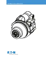
X70
Brand: Eaton Pages: 24
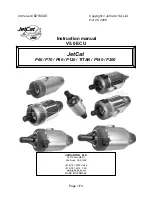
P60
Brand: JetCat Pages: 74
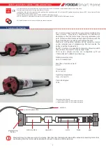
35EV/S Series
Brand: YOODA Pages: 7

VR Series
Brand: Waukesha Pages: 142


