4-1, Meguro 1-chome, Meguro-ku, Tokyo 153-8654, Japan
AV RECEIVER/DVD PLAYER 6.5 INCH WIDE DISPLAY
This service manual should be used together with the following manual(s):
DVD Mech. Module:Circuit Description, Mech. Description, Disassembly
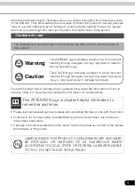
For details, refer to "Important Check Points for Good Servicing".
K-ZZD.MAR. 2005 Printed in Japan
Summary of Contents for AVH-P5750DVD
Page 7: ...AVH P5750DVD RC 7 5 6 7 8 5 6 7 8 C D F A B E 1 SPECIFICATIONS ...
Page 8: ...AVH P5750DVD RC 8 1 2 3 4 1 2 3 4 C D F A B E ...
Page 9: ...AVH P5750DVD RC 9 5 6 7 8 5 6 7 8 C D F A B E ...
Page 12: ...AVH P5750DVD RC 12 1 2 3 4 1 2 3 4 C D F A B E 2 2 EXTERIOR 1 28 88 89 97 ...
Page 14: ...AVH P5750DVD RC 14 1 2 3 4 1 2 3 4 C D F A B E 2 3 EXTERIOR 2 172 172 ...
Page 16: ...AVH P5750DVD RC 16 1 2 3 4 1 2 3 4 C D F A B E 2 4 EXTERIOR 3 ...
Page 18: ...AVH P5750DVD RC 18 1 2 3 4 1 2 3 4 C D F A B E 2 5 DVD MECHANISM MODULE MS3 V1 M ...
Page 42: ...AVH P5750DVD RC 42 1 2 3 4 1 2 3 4 C D F A B E A a B b B a B a B b 1 TOUCH PANEL F CN5001 ...
Page 43: ...AVH P5750DVD RC 43 5 6 7 8 5 6 7 8 C D F A B E A a B b B a B a B b 2 CN171 A 1 2 H CN4301 ...
Page 45: ...AVH P5750DVD RC 45 5 6 7 8 5 6 7 8 C D F A B E B a B b B b 2 LCD MODULE ...
Page 49: ...AVH P5750DVD RC 49 5 6 7 8 5 6 7 8 C D F A B E C b 1 2 C a 1 2 C a 1 2 C b 1 2 ...
Page 53: ...AVH P5750DVD RC 53 5 6 7 8 5 6 7 8 C D F A B E 2 2 C CN181 1 2 A ...
Page 58: ...AVH P5750DVD RC 58 1 2 3 4 1 2 3 4 C D F A B E 3 10 INVERTER PCB F B CN4521 ...
Page 60: ...AVH P5750DVD RC 60 1 2 3 4 1 2 3 4 C D F A B E 3 11 RGB UNIT G CN154 1 2 A ...
Page 61: ...AVH P5750DVD RC 61 5 6 7 8 5 6 7 8 C D F A B E G CN151 G RGB UNIT 1 2 A DIGITAL OUTPUT ...
Page 62: ...AVH P5750DVD RC 62 1 2 3 4 1 2 3 4 C D F A B E 3 12 UPPER PCB H B CN4591 ...
Page 64: ...AVH P5750DVD RC 64 1 2 3 4 1 2 3 4 C D F A B E 3 13 KEYBOARD UNIT I ...
Page 65: ...AVH P5750DVD RC 65 5 6 7 8 5 6 7 8 C D F A B E I CN101 I KEYBOARD UNIT 1 2 A ...
Page 73: ...AVH P5750DVD RC 73 5 6 7 8 5 6 7 8 C D F A B E B SIDE A LCD MODULE ONT 71 F CN5001 ...
Page 75: ...AVH P5750DVD RC 75 5 6 7 8 5 6 7 8 C D F A B E B SIDE B CVBS1 V14 V33 V8 V25 5 YSIN ...
Page 77: ...AVH P5750DVD RC 77 5 6 7 8 5 6 7 8 C D F A B E C SIDE A IC Q PICKUP UNIT SERVICE M M3 A CN151 ...
Page 78: ...AVH P5750DVD RC 78 1 2 3 4 1 2 3 4 C D F A B E C C DVD CORE UNIT IC Q ...
Page 79: ...AVH P5750DVD RC 79 5 6 7 8 5 6 7 8 C D F A B E C SIDE B D ...
Page 87: ...AVH P5750DVD RC 87 5 6 7 8 5 6 7 8 C D F A B E J J MAIN UNIT SIDE B ...
Page 117: ...AVH P5750DVD RC 117 5 6 7 8 5 6 7 8 C D F A B E Circuit Diagram 1 ...
Page 119: ...AVH P5750DVD RC 119 5 6 7 8 5 6 7 8 C D F A B E Circuit Diagram 2 ...
Page 122: ...AVH P5750DVD RC 122 1 2 3 4 1 2 3 4 C D F A B E Circuit Diagram 3 ...
Page 195: ...AVH P5750DVD RC 195 5 6 7 8 5 6 7 8 C D F A B E 8 OPERATIONS ...
Page 196: ...AVH P5750DVD RC 196 1 2 3 4 1 2 3 4 C D F A B E ...
Page 197: ...AVH P5750DVD RC 197 5 6 7 8 5 6 7 8 C D F A B E ...
Page 198: ...AVH P5750DVD RC 198 1 2 3 4 1 2 3 4 C D F A B E ...
Page 199: ...AVH P5750DVD RC 199 5 6 7 8 5 6 7 8 C D F A B E ...
Page 200: ...AVH P5750DVD RC 200 1 2 3 4 1 2 3 4 C D F A B E ...
Page 201: ...AVH P5750DVD RC 201 5 6 7 8 5 6 7 8 C D F A B E ...
Page 202: ...AVH P5750DVD RC 202 1 2 3 4 1 2 3 4 C D F A B E ...
Page 203: ...AVH P5750DVD RC 203 5 6 7 8 5 6 7 8 C D F A B E ...
Page 204: ...AVH P5750DVD RC 204 1 2 3 4 1 2 3 4 C D F A B E ...
Page 205: ...AVH P5750DVD RC 205 5 6 7 8 5 6 7 8 C D F A B E ...
Page 206: ...AVH P5750DVD RC 206 1 2 3 4 1 2 3 4 C D F A B E ...
Page 207: ...AVH P5750DVD RC 207 5 6 7 8 5 6 7 8 C D F A B E ...
Page 208: ...AVH P5750DVD RC 208 1 2 3 4 1 2 3 4 C D F A B E ...
Page 209: ...AVH P5750DVD RC 209 5 6 7 8 5 6 7 8 C D F A B E ...
Page 210: ...AVH P5750DVD RC 210 1 2 3 4 1 2 3 4 C D F A B E ...
Page 211: ...AVH P5750DVD RC 211 5 6 7 8 5 6 7 8 C D F A B E ...