background image

Published by SaS/WS 1065 BU TV Consumer Care, the Netherlands

Subject to modification

EN 3122 785 18842

2010-Jun-25

©

Copyright 2010 Koninklijke Philips Electronics N.V.

All rights reserved. No part of this publication may be reproduced, stored in a 
retrieval system or transmitted, in any form or by any means, electronic, mechanical, 
photocopying, or otherwise without the prior permission of Philips.

Colour Television

Chassis

TPM5.2E

LA

1

88

40_000_100

3

22.ep

s


100

3

22 

Contents

Page

1.

Revision List

2

2.

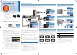
Technical Specifications, Connections

2

3.

Precautions, Notes, and Abbreviation List

5

4.

Mechanical Instructions

9

5.

Service Modes, Error Codes, and Fault Finding 14

6.

Alignments

19

7.

Circuit Descriptions

22

8.

IC Data Sheets

25

9.

Block Diagrams

Wiring Diagram 19", 22"

31

Wiring Diagram 26"

32

Block Diagram

33

10.

Circuit Diagrams and PWB Layouts

Drawing PWB

Power Board: 19", 22"

(A01)

34

35-36

Power Board: 26"

(A01)

37

38-39

SSB: Power-1

(B01)

40

53-54

SSB: Power-2

(B02)

41

53-54

SSB: Tuner

(B03)

42

53-54

SSB: MT5363 By-pass/Trap

(B04)

43

53-54

SSB: MT5363 peripheral/USB2.0

(B05)

44

53-54

SSB: DDR2 memory

(B06)

45

53-54

SSB: Flash/JTAG/UART/IR

(B07)

46

53-54

SSB: CI card

(B08)

47

53-54

SSB: Scart1/Scart2

(B09)

48

53-54

SSB: YPbPr/VGA input

(B10)

49

53-54

SSB: HDMI 1/ HDMI 2

(B11)

50

53-54

SSB: Audio Amp/Headphone out

(B12)

51

53-54

SSB: LVDS output

(B13)

52

53-54

IR/LED Board

(J)

55

56

11.

Styling Sheets

Styling Sheet 19"

57

Styling Sheet 22"

58

Styling Sheet 26"

59

Summary of Contents for 19PFL3405H/05

Page 1: ... 5 Service Modes Error Codes and Fault Finding 14 6 Alignments 19 7 Circuit Descriptions 22 8 IC Data Sheets 25 9 Block Diagrams Wiring Diagram 19 22 31 Wiring Diagram 26 32 Block Diagram 33 10 Circuit Diagrams and PWB Layouts Drawing PWB Power Board 19 22 A01 34 35 36 Power Board 26 A01 37 38 39 SSB Power 1 B01 40 53 54 SSB Power 2 B02 41 53 54 SSB Tuner B03 42 53 54 SSB MT5363 By pass Trap B04 4...

Page 2: ...to the different set executions Specifications are indicative subject to change 2 1 Technical Specifications For on line product support please use the links in Here is product information available as well as getting started user manuals frequently asked questions and software drivers Table 2 1 Described Model Numbers Note The given Model Numbers are subject to change 2 2 Directions for Use Direc...

Page 3: ...y Rd Red Wh White Ye Yellow 2 3 1 Side Connections 1 Common Interface 68p See diagram B08 SSB CI card jk 2 Cinch Audio In Ye Video CVBS 1 VPP 75 Ω jq Rd Audio R 0 5 VRMS 10 kΩ jq Wh Audio L 0 5 VRMS 10 kΩ jq 3 USB2 0 Figure 2 2 USB type A 1 5V k 2 Data jk 3 Data jk 4 Ground Gnd H 4 Head phone Output Bk Head phone 80 600 Ω 10 mW ot 1 6 2 3 4 5 7 8 9 11 12 10 13 18840_001_100323 eps 100428 1 2 3 4 1...

Page 4: ...1 kΩ k 4 Ground Audio Gnd H 5 Ground Blue Gnd H 6 Audio L 0 5 VRMS 10 kΩ j 7 Video Blue C out 0 7 VPP 75 Ω jk 8 Function Select 0 2 V INT 4 5 7 V EXT 16 9 9 5 12 V EXT 4 3 j 9 Ground Green Gnd H 10 n c 11 Video Green 0 7 VPP 75 Ω j 12 n c 13 Ground Red Gnd H 14 Ground P50 Gnd H 15 Video Red C 0 7 VPP 75 Ω j 16 Status FBL 0 0 4 V INT 1 3 V EXT 75 Ω j 17 Ground Video Gnd H 18 Ground FBL Gnd H 19 Vid...

Page 5: ...475 25 MHz for PAL or 61 25 MHz for NTSC channel 3 Where necessary measure the waveforms and voltages with D and without E aerial signal Measure the voltages in the power supply section both in normal operation G and in stand by F These values are indicated by means of the appropriate symbols 3 3 2 Schematic Notes All resistor values are in ohms and the value multiplier is often used to indicate t...

Page 6: ...e dangerous in themselves they can cause unexpected reactions that are best avoided Before reaching into a powered TV set it is best to test the high voltage insulation It is easy to do and is a good service precaution 3 4 Abbreviation List 0 6 12 SCART switch control signal on A V board 0 loop through AUX to TV 6 play 16 9 format 12 play 4 3 format AARA Automatic Aspect Ratio Adaptation algorithm...

Page 7: ...ational Telecommunication Union relating to radio communication ITU 656 a k a SDI is a digitized video format used for broadcast grade video Uncompressed digital component or digital composite signals can be used The SDI signal is self synchronizing uses 8 bit or 10 bit data words and has a maximum data rate of 270 Mbit s with a minimum bandwidth of 135 MHz ITV Institutional TeleVision TV sets for...

Page 8: ... I2C SCL F CLock Signal on Fast I2 C bus SD Standard Definition SDA Serial Data I2C SDA F DAta Signal on Fast I2 C bus SDI Serial Digital Interface see ITU 656 SDRAM Synchronous DRAM SECAM SEequence Couleur Avec Mémoire Color system mainly used in France and East Europe Color carriers 4 406250 MHz and 4 250000 MHz SIF Sound Intermediate Frequency SMPS Switched Mode Power Supply SoC System on Chip ...

Page 9: ...ex of this chapter 4 1 Cable Dressing 4 2 Service Positions 4 3 Assembly Panel Removal 4 4 Set Re assembly Notes Figures below can deviate slightly from the actual situation due to the different set executions 4 1 Cable Dressing Figure 4 1 Cable dressing 19 18840_101_100324 eps 100324 ...

Page 10: ...Mechanical Instructions EN 10 TPM5 2E LA 4 2010 Jun 25 Figure 4 2 Cable dressing 22 18840_102_100324 eps 100324 ...

Page 11: ...structions below apply to the 19PFL3405H xx but are similar for other models 4 3 1 Rear Cover Warning Disconnect the mains power cord before removing the rear cover 1 Remove the fixation screws that secure the stand at the bottom of the stand Then remove the stand 2 Remove fixation screws 1 2 and 3 that secure the rear cover see Figure 4 4 3 The rear cover is secured with locking clips at the side...

Page 12: ...ive replace the whole unit 4 3 4 Speakers 1 Release the speaker cable from its clamps 2 Unplug the speaker connector from the SSB 3 Take the speakers out When defective replace the whole unit 4 3 5 Stand removal Caution it is mandatory to remount all different screws at their original position during re assembly Be sure to put the set in the Service Position 1 Remove the speaker cables as describe...

Page 13: ...anel with the bezel 7 Lift the LCD Panel from the bezel 8 Remove the fixation screws that secure the panel with the Metal frame 9 Take the panel out Remove the Flat Foil connector from the panel When defective replace the whole unit 4 4 Set Re assembly To re assemble the whole set execute all processes in reverse order Notes While re assembling make sure that all cables are placed and connected in...

Page 14: ...CSM Menu 3 How to Navigate By means of the CURSOR DOWN UP knob or the scroll wheel on the RC transmitter can be navigated through the menus General 1 1 Set Type NVM read write max 16 characters 1 2 Production code NVM read write max 16 characters 1 3 Installation date Date the software was installed 1 4 Option Code Store in NVM set feature grouping as option panel code 1 5 Codes Error code Layer 2...

Page 15: ...s de pends on the input 15 ADC_Gain_B 0 255 79 0 87 Analogue to Digital Converter Gain for Blue AutoColor affects this and it value is depends on the input 16 ADC_Offset_R 0 255 113 128 113 Analogue to Digital Converter Offset for Red AutoColor affects this and it value is de pends on the input 17 ADC_Offset_G 0 255 109 128 109 Analogue to Digital Converter Offset for Green AutoColor affects this ...

Page 16: ...e cable for TPM5 2x xx 3122 785 90630 Note While having problems contact the local support desk 39 AUD_LIPSYNC_SPDIF 272 272 200 200 200 Audio delay to the S P DIF output is delay is ahead NVM value Delay ms 0 147 40 Tuner_ID 95 95 95 Tuner Identification 94 NXP 95 LG 41 OPT AV2 Scart2 0 2 0 0 0 0 not available 2 CVBS YC 42 OPT HDMI2 0 1 0 0 1 On Off 43 OPT Reset Option 0 1 Press OK Press OK Press...

Page 17: ...upport 2 Find information and software related to your TV 3 Select the latest software update file and download it to your PC 4 Insert a USB flash drive into one of the USB ports of your PC 5 Decompress the downloaded ZIP file and copy the autorun upg to the root directory of the USB flash drive 5 3 4 Update the TV software 1 Insert the USB flash drive that contains the software update file 2 Then...

Page 18: ...eft side and all other errors shift one position to the right Basically there are three kinds of error codes 5 5 Fault Finding and Repair Tips 5 5 1 Speakers Make sure that the volume is set to minimum during disconnecting the speakers in the ON state of the TV The audio amplifier can be damaged by disconnecting the speakers during ON state of the set 5 5 2 Tuner Attention In case the tuner is rep...

Page 19: ...r pattern by signal generator 4 Enter factory mode menu press numeric keys 062596 INFO key FAC mode menu Alignment 1 At SAM mode menu select AUTO_COLOR item Then press OK key to adjust ADC_GAIN_R ADC_GAIN_G ADC_GAIN_B and ADC_OFFSET_R ADC_OFFSET_G ADC_OFFSET_B Then store those values to NVM 2 Apply 100 white pattern 3 Set colour temperature to NORMAL 4 At FAC mode menu adjust the CLR TEMP R CLR TE...

Page 20: ...768 60 Hz PC mode with five white block pattern Figure 6 1 Five white blocks pattern Input Signal Strength 0 7 Vp p linear voltage Input Injection Point PC D SUB input 6 4 3 Alignment method Initial Set up 1 Select source as PC 2 Set Contrast 50 Sharp and Brightness 50 Sharp at normal menu mode 3 Apply 5 white block pattern by VGA pattern generator see Figure 6 1 4 Enter factory mode menu press nu...

Page 21: ...5H 12_2 AUO M185XW01 V6 122 19PFL3405H 05_1 LG LC185EXN SCA1 119 22PFL3405H 12_1 LG LC216EXN SCA1 120 22PFL3405H 12_2 CMO V216B1 LE1 123 22PFL3405H 05_1 LG LC216EXN SCA1 120 26PFL3405H 12_1 LG LC260EXN SCB1 121 26PFL3405H 12_2 AUO T260XW06 V1 124 26PFL3405H 05_1 LG LC260EXN SCB1 121 22PFL3415H 12_1 LG LC216EXN SCA1 120 22PFL3415H 60_1 LG LC216EXN SCA1 120 19HFL3232D 10_1 LG LC185EXN SCA1 119 22HFL...

Page 22: ...arate drawing for clarification 7 1 Introduction The TPM5 2E LA chassis is using the MT5363 main processor 7 1 1 TPM5 2E Architecture Overview For details about the chassis block diagrams refer to chapter 9 Block Diagrams An overview of the TPM5 1E LA architecture can be found in Figure 7 1 Figure 7 1 Architecture of TPM5 2E LA 64 MB DDR2 2 NAND Flash 16MB 24C64 NVM SPI 24C02 HDMI EDID REAR HDMI T...

Page 23: ...3 TPM5 2E LA 7 2010 Jun 25 7 1 2 SSB Cell Layout Figure 7 2 SSB layout cells top view 18840_206_100406 eps 100428 AUDIO CLASS D DC DC TUNER ANALOG I O SERVICE CONNECTOR MT5363 DIGITAL I O COMMON INTERFACE ANALOG I O DIGITAL I O ...

Page 24: ...288 V 2 1 _ R W P V 5 _ R W P _ B T S 4 2 2 D 3 1 1 3 A P T P M A o i d u A 1 5 7 U F U 3 6 T 3 0 9 G 1 0 7 U 3 0 4 9 P M K C U B t i u c r i C C L 0 5 7 U F U 3 4 T 3 3 7 1 1 1 G r o t a l u g e R A 1 3 3 V D 3 3 V A R D D _ 8 1 V D p i h C n i a M C D o t C D o i d u A L E N A P B S 3 3 V D W S _ V 5 B S R W P O R E N U T _ V 5 Y B D N A T S 4 0 7 Q 1 2 4 4 N O A S O M C 2 0 7 U 3 1 L D 7 1 1 1 ...

Page 25: ...401 Figure 8 1 Internal block diagram 18850_300_100107 eps 100222 Block diagram DVB T ATD CVBS YC Input VADCx4 TV Decoder HDMI Rx HDMI In I F Audio Demod Audio Input Audio ADC Panel LVDS CVBS VDAC TVE DDR DRAM Controller ARM BIM TS Demux VDO In PreProc MDDi Audio In JPEG MPEG H 264 2 D Graphic Mix andPost Processing OSD scaler Vplane scaler PIP Audio DSP IO Bus Standby uP CKGEN Audio I F Audio DAC...

Page 26: ...S1 RDQ0 RDQ7 VCC2IO MEMTP RA6 RVREF RDQ25 RDQ27 RDQ31 VCC2IO GPIO40 VCCK VCCK VCCK PDD4 PDD5 RDQS0_ DVSS DVSS DVSS RVREF DVSS VCCK VCCK PDD6 PDD7 RDQS0 DVSS DVSS DVSS AVSS12_U SB AVSS33_U SB AVSS33_U SB RDQ14 RDQM1 RDQM0 DVSS AVDD12_U SB USB_VRT USB_DM USB_DP RDQ11 RDQ9 RDQ6 RDQ1 AVDD33_U SB AVDD12_H DMI AVSS33_U SB RDQ12 VCC2IO VCC2IO RDQ3 VCCK HDMI_SCL 2 AVSS33_H DMI RX2_C RX2_CB VCC2IO VCC2IO V...

Page 27: ...L2 TUNER_CL K U1RX AR3 N AOSDATA2 P R VCXO T U AL3 V DVSS DVSS VCCK AVDD33_R EF_AADC VCCIO33 VCCIO33 VCCIO33 W DVSS DVSS DVSS DVSS DVSS DVSS VCCK VCCK VCCK AVSS33_R EF_AADC VMID_AAD C AVDD33_A ADC AIN1_L_AA AIN4_L_AA DC AVSS33_A ADC AIN4_R_A AIN5_L_AA DC AIN5_R_A ADC AIN2_R_A AIN6_L_AA DC AIN6_R_A ADC Y AA AIN3_R_A DVSS VCCK DVSS DVSS VCCK DVSS DVSS DVSS DVSS AVDD12_T VDPLL AVDD12_A DC AIN1_R_A AD...

Page 28: ... 100406 Block diagram Pinning information BS IN SW GND SS EN COMP FB CONNECT EXPOSED PAD AND GND PIN TO A CERTAIN GROUND PLANE 1 2 3 4 8 7 6 5 TOP VIEW INTERNAL REGULATORS IN EN ERROR AMPLIFIER 6υA 1 2V OVP RAMP CLK 0 8V 0 3V CURRENT COMPARATOR CURRENT SENSE AMPLIFIER 0 95V SHUTDOWN COMPARATOR COMP SS FB GND OSCILLATOR 340KHz S R Q SW BS IN 5V OVP IN 3 95V Q 1 3 V ...

Page 29: ...Block diagram Pinning information Click and Pop Suppression HPVDD HPVSS HPVDD HPVSS Charge Pump INR INR INL INL OUTL OUTR CPP CPN HPVSS G0 EN Thermal Protection Gain Select G1 VDD Supply Control PGND SGND HPVDD Resistor Array 1 F 1 F 2 2 F Short Circuit Protection Resistor Array HPVDD 1 HPVDD CPP INL INL INR INR PGND CPN 2 3 4 12 11 10 9 16 15 14 13 5 6 7 8 R T U O G0 G1 S S V P H L T U O D N G S ...

Page 30: ... BSPR PVCCR PVCCR PBTL PWP TSSOP PACKAGE TOP VIEW PWM Logic Gate Drive Gate Drive PVCCL PVCCL GVDD PVCCL PVCCL BSPL PGND OUTPL OUTNL PGND GVDD BSNL PWM Logic Gate Drive Gate Drive PVCCL PVCCL GVDD PVCCL PVCCL BSNR PGND OUTNR OUTPR PGND GVDD BSPR LINP LINN RINP RINN UVLO OVLO SC Detect DC Detect Thermal Detect Startup Protection Logic Biases and References FAULT SD GAIN0 PLIMIT AGND AVCC GAIN1 Ramp...

Page 31: ... DV33SB 4 GND 3 RC6 2 LED_G 1 LED_R WIRING DIAGRAM 19 22 Dali SSB 1053 B MAIN POWER SUPPLY 1054 CN902 1 STATUS 2 3 STB 4 24V 5 GND 6 GND 7 GND 8 5 2V 9 5 2V 10 DIM 11 DIM 12 LED ON OFF RIGHT SPEAKER Board Level Repair Component Level Repair Only For Authorized Workshop CN601 1 ROUT 2 ROUT 3 LOUT 4 LOUT A LEFT SPEAKER IR LED BOARD 1056 CN001 4P CN301 7P J CN903 1 24V 2 24V 3 24V 4 24V 5 24V 6 GND 7...

Page 32: ...4 GND 3 RC6 2 LED_G 1 LED_R WIRING DIAGRAM 26 Dali SSB 1053 B MAIN POWER SUPPLY 1054 CN902 1 STATUS 2 3 STB 4 24V 5 GND 6 GND 7 GND 8 5 2V 9 5 2V 10 DIM 11 DIM 12 LED ON OFF RIGHT SPEAKER Board Level Repair Component Level Repair Only For Authorized Workshop CN601 1 ROUT 2 ROUT 3 LOUT 4 LOUT A LEFT SPEAKER IR LED BOARD 1056 CN001 4P CN301 7P J CN903 1 24V 2 24V 3 24V 4 24V 5 24V 6 GND 7 GND 8 GND ...

Page 33: ...I 24C02 HDMI EDID REAR HDMI TUNER NOR Flash 512KB LED LCD Panel CVBS1 24C02 HDMI EDID REAR HDMI SIDE HDMI ADIN4_SRV ADIN2_SRV IF BPF CVBS1 SIDE AV VGA 24C02 VGA EDID OIRI OPCTRL0 R1 G1 B1 Component VDAC_OUT1 HP AMP TPA6132A2 Audio AMP TPA3113D2 SCART AR0 AL0 SCART MP3 JPEG S W upgrade NVM clone AR0 AL0 DRV603 CI card IN TTL LVDS ...

Page 34: ... 330 OHM 1 4W NC R933 1K 1 4W 5 NC R933 1K 1 4W 5 NC C925 100PF 1KV C925 100PF 1KV J910 JUMPER NC J910 JUMPER NC 1 2 C927 100N 50V C927 100N 50V F901 FUSE F901 FUSE R903100 OHM 1 4W R903100 OHM 1 4W R904100 OHM 1 4W R904100 OHM 1 4W C904 2 2nF 100V C904 2 2nF 100V R900 2M4 5 1 2W R900 2M4 5 1 2W R942 1KOHM 5 2WS NC R942 1KOHM 5 2WS NC Q904 AO4443 Q904 AO4443 S 1 S 2 S 3 G 4 D 8 D 7 D 6 D 5 ZD903 U...

Page 35: ...03 L904 H5 D905 C903 CN901 J903 L902 R925 RV902 SG902 SG901 C922 C914 H6 FB901 C906 C900 C901 J910 BD901 H4 F901 Q903 J904 FB903 J915 L905 C923 CN902 CN903 C924 R937 D903 FB905 J909 J905 J906 J912 C935 SG904 SG903 H2 C907 R942 D908 R945 J919 FB906 J920 FB907 J914 FB908 FB909 HD905 C909 D906 D907 R946 C931 C920 J901 C905 ZD902 J921 J922 FB902 FB904 J902 J907 J913 R929 C930 R933 R939 C938 T901 IC903...

Page 36: ...FD2 R904 R903 R916 R917 R927 R931 R919 R909 R923 R926 R928 R932 R910 R915 R908 C917 C919 C926 C951 C927 C928 C910 C912 C929 C933 R905 R921 R902 R901 R907 R922 R920 R936 D904 ZD903 ZD904 C902 C904 C911 C918 R934 Q901 R914 C916 J916 J918 J917 C936 C937 R940 R941 R944 Q904 R911 R906 Q902 C932 C934 R924 R930 R935 R918 Q906 C939 Q905 IC901 ...

Page 37: ... C954 1000uF 10V C954 1000uF 10V R932 680R 1 8W 1 R932 680R 1 8W 1 IC905 TNY277PN TL IC905 TNY277PN TL EN UV 1 BP M 2 D 4 S 5 S 6 S 7 S 8 C922 470uF 16V C922 470uF 16V L903 3 5uH L903 3 5uH FB906 BEAD FB906 BEAD 1 2 R938 68 OHM 1 4W R938 68 OHM 1 4W R956 11K 1 8W 1 R956 11K 1 8W 1 CN902 Wire Harness CN902 Wire Harness 1 2 3 4 5 6 7 8 9 10 11 12 13 14 SG901 SPG 201M LF SG901 SPG 201M LF SG903 SPG 2...

Page 38: ... J906 D920 ZD912 J905 G1 C904 C945 C929 IC905 R922 H4 HD902 L903 L904 L905 T902 L906 HQ903 D909 Q903 R900 SG903 SG904 HD909 FB905 J917 J904 ZD913 D915 R953 R945 D917 R929 ZD915 J903 J910 J908 F901 D907 CN902 J907 ZD902 J922 J921 J920 FB903 J919 FB901 J911 J914 J912 J913 G2 G3 G4 C936 ZD908 R911 R935 ZD906 D908 D910 D905 C907 D902 CN903 C908 D901 R933 D916 ZD910 L902 T901 BD901 C905 C906 C909 C900 ...

Page 39: ...8 C932 C947 C952 R918 R919 R923 R926 R927 R931 R932 R907 R940 R941 R944 R947 R955 R957 R970 R903 R904 R916 R917 Q907 Q909 R909 C953 R956 C916 Q901 C925 C931 R915 R906 Q906 R920 C933 R924 R951 R942 C930 D904 ZD903 ZD909 C911 C918 ZD907 R908 R913 R902 R939 C902 C938 C939 R905 R910 R914 R938 C958 R912 Q910 R930 R965 R943 R936 R934 ZD904 R921 R937 C941 R946 R948 Q911 R928 J924 IC901 ...

Page 40: ...17 120R 1 1 10W CN701 CONN CN701 CONN 1 2 3 4 5 6 7 8 9 10 11 12 13 C726 NC 100N 16V C726 NC 100N 16V C701 22uF 10V C701 22uF 10V R716 47K1 16W R716 47K1 16W C719 10uF 16V C719 10uF 16V R703 NC 10K 1 4W R703 NC 10K 1 4W R710 NC 4 7K1 16W R710 NC 4 7K1 16W L701 15uH L701 15uH R738 NC 0R05 1 4W R738 NC 0R05 1 4W FB707 NC 220R 2000mA FB707 NC 220R 2000mA 1 2 Q706 NC BC847C Q706 NC BC847C 3 2 1 C725 N...

Page 41: ... C765 10uF 16V C763 1UF16V C763 1UF16V C762 100uF 10V C762 100uF 10V C752 100uF 16V C752 100uF 16V R755 33K 1 10W R755 33K 1 10W R750 10K 1 10W R750 10K 1 10W R765 0R05 1 10W R765 0R05 1 10W R762 1K 1 16W 1 R762 1K 1 16W 1 C755 100uF 16V C755 100uF 16V C764 100uF 16V C764 100uF 16V R753 NC 10K 1 10W R753 NC 10K 1 10W C723 100N 16V C723 100N 16V U751 IC G903T63UF 0 6A 3 3V SOT 223 U751 IC G903T63UF...

Page 42: ...A FB1015 NC 120R 3000mA 1 2 R1001 NC 75OHM1 16W R1001 NC 75OHM1 16W L1009 NC 0 22uH 10 L1009 NC 0 22uH 10 R1012 300R 1 10W 1 R1012 300R 1 10W 1 C1097 NC 10N 50V C1097 NC 10N 50V R1028 NC 0R05 1 10W R1028 NC 0R05 1 10W FB1022 120R 3000mA FB1022 120R 3000mA 1 2 R1018 NC 0R05 1 16W R1018 NC 0R05 1 16W R1076 NC 0R05OHM1 16W R1076 NC 0R05OHM1 16W C1096 NC 100N 16V C1096 NC 100N 16V R1037 NC 4 7K1 16W R...

Page 43: ..._TVDPLL AF29 AVDD12_SYSPLL AG32 AVDD12_ADCPLL AH33 AVDD12_APLL AG30 DVSS Y3 DVSS J4 DVSS L4 DVSS W4 DVSS J6 DVSS L6 DVSS W6 DVSS C8 DVSS E8 DVSS G8 DVSS AE8 DVSS D9 DVSS F9 DVSS AF9 DVSS G10 DVSS AB13 DVSS AD13 DVSS N14 DVSS R14 DVSS W14 DVSS AC14 DVSS P15 DVSS T15 DVSS V15 DVSS AB15 DVSS U16 DVSS W16 DVSS AA16 DVSS AC16 DVSS T17 DVSS V17 DVSS Y17 DVSS AB17 DVSS R18 DVSS U18 DVSS W18 DVSS AA18 DVS...

Page 44: ...B37 AVICM AF35 AR1 V33 AIN6_L_AADC AA36 AIN3_L_AADC AC36 AL0 AF37 AVSS33_DIG AJ30 AVSS33_SIF AK29 AVDD33_DIG AK31 AVDD33_SIF AL30 AF AM33 MPXN AN36 MPXP AN34 ALIN L32 AOLRCK M37 AOSDATA3 K31 ASPDIF K33 AOBCK L34 AOSDATA4 N32 AOSDATA1 P35 AOSDATA0 L36 AOMCLK M35 AOSDATA2 P37 C4065 NC 10U 16V C4065 NC 10U 16V TP4050 TP4050 1 D4050 BAV99 D4050 BAV99 3 1 2 C4058 100N 16V C4058 100N 16V R4053 NC 4 7K1 ...

Page 45: ... 16W 5 1 2 3 4 8 7 6 5 RP4104 56R 1 16W 5 RP4104 56R 1 16W 5 1 2 3 4 8 7 6 5 C4118 100N 16V C4118 100N 16V C4110 NC 10U 16V C4110 NC 10U 16V C4127 100N 16V C4127 100N 16V R4110 22 OHM 1 16W R4110 22 OHM 1 16W R4107 100OHM1 16W R4107 100OHM1 16W C4106 100N 16V C4106 100N 16V C4112 100N 16V C4112 100N 16V C4111 1UF 16V C4111 1UF 16V C4104 100N 16V C4104 100N 16V R4111 22 OHM 1 16W R4111 22 OHM 1 16W...

Page 46: ...OHM1 16W R4193 0R05OHM1 16W R4190 4 7K1 16W R4190 4 7K1 16W R4189 4 7K1 16W R4189 4 7K1 16W U410 MAX809STRG U410 MAX809STRG GND 1 RESET 2 VCC 3 R4230 NC 0R05OHM1 16W R4230 NC 0R05OHM1 16W FB4152 600R 200mA FB4152 600R 200mA 1 2 R4166 10K1 16W R4166 10K1 16W R4186 4 7K1 16W R4186 4 7K1 16W TP4151 TP4151 1 R4161 NC 1K 1 10W R4161 NC 1K 1 10W U409 M24C64 WDW6TP U409 M24C64 WDW6TP E0 1 E1 2 E2 3 VSS 4...

Page 47: ...15 41 CE2 42 RFSH 43 RFU 44 RFU 45 A17 46 A18 47 A19 48 A20 49 A21 50 VCC 51 VPP2 52 A22 53 A23 54 A24 55 A25 56 RFU 57 RESET 58 WAIT 59 RFU 60 REG 61 69 69 70 70 71 71 72 72 R4202 22 OHM 1 16W R4202 22 OHM 1 16W R4217 22 OHM 1 16W R4217 22 OHM 1 16W R4225 10K1 16W R4225 10K1 16W C4205 10P 50V C4205 10P 50V R4209 22 OHM 1 16W R4209 22 OHM 1 16W C4206 10P 50V C4206 10P 50V R4226 10K1 16W R4226 10K1...

Page 48: ...Q1050 DTC623TK R1 Q1050 DTC623TK 2 3 1 C1078 10N 50V C1078 10N 50V ZD1065 NC VPORT0603100KV05 ZD1065 NC VPORT0603100KV05 1 2 R1134 10K1 16W R1134 10K1 16W R1063 68OHM 1 16W R1063 68OHM 1 16W U108 L78L12ABUTR U108 L78L12ABUTR IN 3 OUT 1 GND 2 R1139 5K1 1 16W 5 R1139 5K1 1 16W 5 R1068 33K 1 16W R1068 33K 1 16W R1129 75 OHM 1 10W R1129 75 OHM 1 10W R1077 33K 1 16W R1077 33K 1 16W ZD1051 NC VPORT06031...

Page 49: ...mA FB1168 600R 200mA 1 2 R1177 0R05OHM1 16W R1177 0R05OHM1 16W R1209 NC 0R05OHM1 16W R1209 NC 0R05OHM1 16W A B C CN116 JACK A B C CN116 JACK 2 1 4 3 5 6 R1163 10K1 16W R1163 10K1 16W R1169 56R 1 16W 1 R1169 56R 1 16W 1 FB1172 BEAD FB1172 BEAD 1 2 R1184 1 5K 1 16W R1184 1 5K 1 16W C1197 15PF50V C1197 15PF50V CN104 88G 35315FVCL CN104 88G 35315FVCL 1 6 2 7 3 8 4 9 5 11 12 13 14 15 10 17 16 18 19 R11...

Page 50: ...19 HDMI_SDA2 AL14 PWR5V_2 AM15 HDMI_HPD2 AN16 HDMI_SCL1 AM17 HDMI_HPD1 AL18 HDMI_SDA1 AN18 AVSS12_USB AM9 AVDD12_USB AL10 AVDD33_USB AM11 USB_VRT AN10 USB_DP AU10 USB_DM AR10 PWR5V_1 AL16 AVSS33_USB AP9 AVSS33_USB AT9 AVSS33_USB AT11 ZD503 NC VPORT0603100KV05 ZD503 NC VPORT0603100KV05 1 2 U507 NC RClamp0524P TCT U507 NC RClamp0524P TCT IN1 1 IN2 2 GND 3 IN3 4 IN4 5 OUT4 6 OUT3 7 GND 8 OUT2 9 OUT1 ...

Page 51: ... R636 100OHM1 16W R629 NC 100K1 16W R629 NC 100K1 16W C625 330N 25V C625 330N 25V R645 0R05OHM1 16W R645 0R05OHM1 16W C641 1N 50V C641 1N 50V R628 NC 47K1 16W R628 NC 47K1 16W D609 BAS316 D609 BAS316 A 1 K 2 C613 100N 50V C613 100N 50V C624 1UF16V C624 1UF16V U601 TPA3113D2 U601 TPA3113D2 SDZ 1 FAULTZ 2 LINP 3 LINN 4 GAIN0 5 GAIN1 6 AVCC 7 AGND 8 GVDD 9 PLIMIT 10 RINN 11 RINP 12 NC 13 PBTL 14 PVCC...

Page 52: ...18 AVDD33_LVDS H15 AVDD12_VPLL N18 AOCKP C18 AOCKN A18 AECKP H19 AECKN F19 AVSS12_VPLL P19 AO3P D19 AO3N B19 AE3P G20 AE3N E20 AO4P C20 AO4N A20 AE4P H21 AE4N F21 TP_VPLL M19 R409 4 7K 1 10W R409 4 7K 1 10W R417 0R05 1 10W R417 0R05 1 10W C401 NC 47uF 6 3V C401 NC 47uF 6 3V R406 1K1 10W R406 1K1 10W TP419 TP419 1 FB403 NC 120R 3000mA FB403 NC 120R 3000mA 1 2 CN408 Wafer 2 15P 2 0picth NC CONN CN40...

Page 53: ...01 L1002 L1003 L1005 L4150 FB611 FB402 FB403 FB1011 FB1012 FB1022 FB1167 FB1168 FB406 FB1008 FB1009 FB1014 FB1016 FB1017 L1008 L1009 FB608 FB705 FB706 FB1006 FB4200 FB4060 FB607 FB609 FB610 L602 L601 L603 L604 U602 U101 R616 R714 R4109 R4110 R4106 R4111 R4112 R4107 R4051 R4052 R608 R610 R1001 R1000 R1002 R1003 R1005 R1007 R1010 R1024 R1029 R1030 R1135 R1137 R1138 R1060 R1062 R1063 R1064 R1065 R106...

Page 54: ...019 FB612 FB613 FB614 FB615 FB1003 FB1004 FB1015 FB617 FB605 FB606 U603 R4108 R643 R1006 R1008 R1061 R1072 R1084 R1087 R4002 R4165 R4166 R4167 R4168 R4170 R4180 R4184 R4194 R4203 R4205 R4222 R4223 R4224 R4225 R4226 R4227 R4228 R4231 R507 R508 R509 R510 R511 R512 R515 R516 R517 R540 R541 R542 R505 R506 R1131 R1134 R636 R4164 R4169 R4174 R4177 R530 R620 R4006 R4199 R1081 R1016 R1021 R653 R654 R671 Q...

Page 55: ...F45 U201 IRM 3636F45 VS 3 OUT 1 GND 2 LED302 LED LED302 LED 1 2 TP1 TP1 1 Q301 BC847C Q301 BC847C R304 1K 1 10W R304 1K 1 10W R203 100 OHM 1 10W R203 100 OHM 1 10W TP3 TP3 1 TP4 TP4 1 TP6 TP6 1 R201 2K7 1 10W 5 R201 2K7 1 10W 5 CN301 S1315 07RVB S01 K CN301 S1315 07RVB S01 K 1 2 3 4 9 8 5 6 7 CN001 CN001 1 2 3 4 5 R301 6 2K 1 10W R301 6 2K 1 10W TP5 TP5 1 C201 22U 10V C201 22U 10V C201 C4 CN001 C1...

Page 56: ...2E LA 10 Circuit Diagrams and PWB Layouts 2010 Jun 25 Layout IR LED Board 18840_522_100408 eps 100428 C201 R201 R203 R301 R304 TP1 TP3 TP4 TP5 TP6 H13 FD6 Q301 CN301 H11 H12 CN001 ZD202 SPG1 LED302 U201 Top Bottom ...

Page 57: ...11 Styling Sheets Styling Sheet 19 18840_800_100415 eps 100415 PICO 19 Pos No Description Remarks 30 FRONT CABINET 40 REAR COVER 50 STAND ASSY 91 STAND NECK 1176 REMOTE CONTROL FOR ELECTRICAL PARTS ASSEMBLIES SEE WIRING DIAGRAM CHAPTER 9 30 40 50 91 ...

Page 58: ...0 Jun 25 Styling Sheet 22 18840_801_100415 eps 100426 PICO 22 Pos No Description Remarks 30 FRONT CABINET 40 REAR COVER 50 STAND ASSY 91 STAND NECK 1176 REMOTE CONTROL FOR ELECTRICAL PARTS ASSEMBLIES SEE WIRING DIAGRAM CHAPTER 9 30 50 40 91 ...

Page 59: ...0 Jun 25 Styling Sheet 26 18840_802_100415 eps 100415 PICO 26 Pos No Description Remarks 30 FRONT CABINET 40 REAR COVER 50 STAND ASSY 68 STAND NECK 1176 REMOTE CONTROL FOR ELECTRICAL PARTS ASSEMBLIES SEE WIRING DIAGRAM CHAPTER 9 30 50 40 90 ...

Reviews: