background image

ORDER NO. MD0508312C1
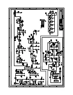
A6

Active Subwoofer System

SB-WA933P

Colour

(S)...Silver Type

1

PDF created with pdfFactory Pro trial version 

www.pdffactory.com

Summary of Contents for SB-WA933

Page 1: ...ORDER NO MD0508312C1 A6 Active Subwoofer System SB WA933P Colour S Silver Type 1 PDF created with pdfFactory Pro trial version www pdffactory com ...

Page 2: ...z 16 dB 38 Hz 190 Hz 10 dB Dimensions W x H x D 285 mm x 402 mm x 520 mm 11 7 32 x 15 13 16 x 20 15 32 Mass 15 kg 33 1 lbs General Power supply AC 120V 60Hz Power consumption 390 W System SC HT933 P Music Center SA HT933 P Satellite Speakers SB HT920 P Active Subwoofer SB WA933 P Note Specifications are subject to change without notice Mass and dimensions are approximate 2 PDF created with pdfFact...

Page 3: ...he original lead dress If a short circuit is found replace all parts which have been overheated or damaged by the short circuit 2 After servicing ensure that all the protective devices such as insulation barriers insulation papers shields are properly installed 3 After servicing check for leakage current to prevent from being 3 PDF created with pdfFactory Pro trial version www pdffactory com ...

Page 4: ...mer from being exposed to a shock hazard 1 1 1 LEAKAGE CURRENT COLD CHECK 1 Unplug the AC cord and connect a jumper between the two prongs on the plug 2 Using an ohmmeter measure the resistance value between the jumpered AC plug and each exposed metallic cabinet part on the equipment such as screwheads connectors control shafts etc When the exposed metallic part has a return path to the chassis th...

Page 5: ...to make the hot checks leakage current must not exceed 1 2 milliamp Should the measurement is outside of the limits specified there is a possibility of a shock hazard and the equipment should be examine and rechecked before it is returned to the customer 1 1 3 Caution for fuse replacement 2 Handling the Lead free Solder 2 1 About lead free solder PbF Distinction of PbF P C B P C B s manufactured u...

Page 6: ...ce The function of this circuitry is to prevent circuitry damage if for example the positive and negative speaker connection wires are shorted or if speaker systems with an impedance less than the indicated rated impedance of the amplifier are used If this occurs follow the procedure outlines below 1 Turn off the power 2 Determine the cause of the problem and correct it 3 Turn on the power once ag...

Page 7: ...ts 2 For reassembly after operation checks or replacement reverse the respective procedures Special reassembly procedures are described only when required 3 Select items from the following index when checks or replacement are required 6 1 Disassembly flow chart The following chart is the procedure for disassembling the casing and inside parts for internal inspection when carrying out the servicing...

Page 8: ...Woofer Speakers 6 1 2 Disassembly of the Power Amp Unit 6 2 Disassembly of the Speaker Unit and Checking of the P C B 6 2 1 Disassembly of the Front Panel Unit 8 PDF created with pdfFactory Pro trial version www pdffactory com ...

Page 9: ... gap between the Front Panel unit and the speaker cabinet assembly unit as arrow shown Steps 2 Slot a piece of wood chip in between the Front Panel unit and the steel ruler as arrow shown 9 PDF created with pdfFactory Pro trial version www pdffactory com ...

Page 10: ...ses which are glued to the unit Step 4 Remove the Front Panel unit from the speaker cabinet assembly unit as arrow shown Assembly of the Front Panel unit Step 1 Clean up the remaining glue at the 8 boss points and replace with the normal glue 10 PDF created with pdfFactory Pro trial version www pdffactory com ...

Page 11: ...back to the speaker cabinet assembly unit 6 2 2 Disassembly of Woofer Speaker Unit 1 Follow Step 1 to Step 4 described in section 6 2 1 Step 1 Remove 4 screws from the Woofer 1 11 PDF created with pdfFactory Pro trial version www pdffactory com ...

Page 12: ...6 2 3 Disassembly of Woofer Speaker Unit 2 Follow Step 1 to Step 4 described in section 6 2 1 Step 1 Remove 4 screws from the Woofer 2 Step 2 Remove the Woofer 2 by detaching the and wires 12 PDF created with pdfFactory Pro trial version www pdffactory com ...

Page 13: ...embly of the Power Amp Unit Step 1 Remove 7 screws from the bottom of the speaker cabinet assembly unit Step 2 Remove 3 screws from the rear panel 13 PDF created with pdfFactory Pro trial version www pdffactory com ...

Page 14: ... the connector CN604 and pull out the entire Power Amp unit 6 2 5 Disassembly of the Rear Panel and Fan Unit Follow Step 1 to Step 4 described in section 6 2 4 Steps 1 and 2 Remove 7 screws from the rear panel 14 PDF created with pdfFactory Pro trial version www pdffactory com ...

Page 15: ...ep 5 Lay the rear panel flat and remove the fan unit as arrow shown 6 2 6 Disassembly and checking of the Amplifier P C B and AC Inlet P C B Follow Step 1 to Step 4 described in section 6 2 4 Follow Step 1 to Step 3 described in section 6 2 5 15 PDF created with pdfFactory Pro trial version www pdffactory com ...

Page 16: ...ow Step 1 to Step 4 described in section 6 2 4 Follow Step 1 to Step 3 described in section 6 2 5 Steps 1 and 2 Remove 4 screws Step 3 Flip the Power P C B as shown for checking both Power P C B and Transformer P C B 6 2 8 Replacement of Power ICs and Transistors 16 PDF created with pdfFactory Pro trial version www pdffactory com ...

Page 17: ...or CP502 Step 2 Remove the AC Inlet P C B by pulling the P C B support claw as arrow shown Step 3 Desolder the terminals of IC601 Transistors Q601 and Q602 Step 4 Disconnect the connectors CN601 CN602 and CN603 and remove the Amplifier P C B Step 5 Remove 4 screws 17 PDF created with pdfFactory Pro trial version www pdffactory com ...

Page 18: ...lopment of the new technology Note The voltage value and waveforms are the reference voltage of this unit measured by DC electronic voltmeter high impedance and oscilloscope on the basis of chassis Accordingly there may arise some error in voltage values and waveforms depending upon the internal impedance of the tester or the measuring unit Importance safety notice Components identified by mark ha...

Page 19: ... parts boxes made of plastics with aluminium foil Put a conductive mat on the work table Ground the soldering iron Do not touch the pins of IC LSI or VLSI with fingers directly 10 Schematic Diagram 10 1 Power Circuit 10 2 AC Inlet Circuit and Transformer Circuit 10 3 Amplifier Circuit 11 Printed Circuit Board 11 1 Power P C B 11 2 AC Inlet P C B and Transformer P C B 11 3 Amplifier P C B 12 Wiring...

Page 20: ...e indications can be used for all areas Capacitor values are in microfarads F unless specified otherwise P Pico farads pF F Farads Resistance values are in ohms unless specified otherwise 1K 1 000 OHM The marking RTL indicates that the Retention Time is limited for this items After the discontinuation of this assembly in production the item will continue to be available for a specific period of ti...

Page 21: ...21 PDF created with pdfFactory Pro trial version www pdffactory com ...

Page 22: ...14 1 2 Cabinet Parts List 22 PDF created with pdfFactory Pro trial version www pdffactory com ...

Page 23: ...OFER SPACER M 20 RMQX0111 EVA PACKING FOR WOOF M 21 XTN26 10JFJ SCREW M 14 2 Electrical Parts List Ref No Part No Part Name Description Remarks PRINTED CIRCUIT BOARD REPX0471E POWER P C B AC INLET P C B TRANSFORMER P C B M RTL REPX0472A AMPLIFIER P C B M RTL INTEGRATED CIRCUITS IC501 RSN311W64D P IC HIC PBF M IC601 RSN312H24A P IC HIC M TRANSISTORS Q501 B1AACF000117 TRANSISTOR M Q502 B1AACF000117 ...

Page 24: ...528 B0EAKM000122 DIODE M D555 B0AACK000004 DIODE M D556 B0BA01100004 DIODE M D557 B0EAKM000117 DIODE M D558 B0AACK000004 DIODE M D559 B0AACK000004 DIODE M D560 B0AACK000004 DIODE M D561 B0BA01100004 DIODE M D562 B0AACK000004 DIODE M D563 B0BA01900005 DIODE M D564 B0BA01900005 DIODE M D565 B0BA01900005 DIODE M D566 B0BA01900005 DIODE M D597 B0FBAM000009 DIODE M D598 B0FBAM000009 DIODE M D599 B0FBAM...

Page 25: ... BACK UP TRANSFORMER M COMPONENT COMBINATION Z501 ERZV10V511CS ZENER M SPEAKER SP1 EAS15PL05B WOOFER UNIT M RELAY RLY501 K6B1AEA00003 RELAY M FUSE F1 K5D602AQ0002 FUSE M FUSE HOLDERS FC501 EYF52BCY FUSE HOLDER M FC502 EYF52BCY FUSE HOLDER M FUSE PROTECTOR FP1 K5G502AA0002 5A FUSE PROTECTOR M HOLDER H503 K1YF15000004 15P WIRE HOLDER M JACKS JK500 K2AB2B000008 JK AC INLET M JK501 K4BC06B00043 JK M J...

Page 26: ...E501 K4CZ01000027 TERMINAL M 26 PDF created with pdfFactory Pro trial version www pdffactory com ...

Page 27: ...K 1 4W M R519 ERDS2TJ824T 820K 1 4W M R520 ERDS2TJ223T 22K 1 4W M R521 ERDS2TJ563T 56K 1 4W M R522 ERDS2TJ563T 56K 1 4W M R523 ERDS2TJ124T 120K 1 4W M R524 ERDS2TJ124T 120K 1 4W M R525 ERDS2TJ154T 150K 1 4W M R526 ERDS2TJ124T 120K 1 4W M R529 ERDS2TJ223T 22K 1 4W M R530 ERD25FVJ1R0T 1 1 4W M R531 ERD25FVJ1R0T 1 1 4W M R532 ERDS2TJ472T 4 7K 1 4W M R533 ERDS1FVJ100T 10 1 2W M R534 ERDS1FVJ100T 10 1 ...

Page 28: ...1 4W M R603 ERDS2TJ103T 10K 1 4W M R604 ERDS2TJ225T 2 2M 1 4W M R606 ERG2SJ220E 22 2W M R609 ERDS1FVJ152T 1 5K 1 2W M R610 ERD2FCVJ4R7T 4 7 1 4W M R611 ERD2FCVJ4R7T 4 7 1 4W M R611 ERDS2TJ103T 10K 1 4W M R612 ERD2FCVJ4R7T 4 7 1 4W M R613 ERDS2TJ272T 2 7K 1 4W M R614 ERDS2TJ272T 2 7K 1 4W M R615 ERDS2TJ473T 47K 1 4W M R616 ERDS2TJ472T 4 7K 1 4W M R617 ERDS2TJ822T 8 2K 1 4W M R618 ERDS2TJ473T 47K 1 ...

Page 29: ... 50V M C533 F1D1H102A012 1000P 50V M C534 ECA1HM330B 33 50V M C543 F1D1H102A012 1000P 50V M C544 ECA1HM101B 100 50V M C545 F1D1H1040002 0 1 50V M C546 F2A1G332A003 3300P 100V M C547 F2A1G472A003 4700P 100V M C548 F2A1G472A003 4700P 100V M C549 F2A1G332A003 3300P 100V M C550 F1D1C103A007 0 01 16V M C551 F1D1H103A046 0 01 50V M C553 ECQE2104KF3 0 1 250V M C554 ECQE1104KF3 0 1 100V M C555 ECEA1VKA4R7...

Page 30: ...3A060 0 01 500V M C611 F1D1H102A012 1000P 50V M C612 F1D1H102A012 1000P 50V M C613 F1B1H103A153 0 01 50V M C614 F1B1H103A153 0 01 50V M C615 F1D1H473A012 0 047 50V M C616 F1D1H473A012 0 047 50V M C619 F1D1H473A012 0 047 50V M C620 F1D1H1040002 0 1 50V M C621 F1D1H1040002 0 1 50V M C647 ECA0JM471B 470 6 3V M C648 F1D1H1040002 0 1 50V M 14 3 Packing Materials Accessories Parts List Ref No Part No Pa...

Page 31: ...FLE0508 P A S E N 31 PDF created with pdfFactory Pro trial version www pdffactory com ...

Page 32: ...01 CN502 JK500 J6010 J6007 J6008 R401 J6006 J6005 D500 R579 J6009 R580 C559 D528 R590 Q519 Q515 Q516 D527 R589 R578 C555 C557 Q517 D525 R587 C556 T502 SUB TRANSFORMER C558 R588 J6001 J6002 J6003 J6004 W1 BRW W2 BLU FC501 FC502 CN503 T501 POWER TRANSFORMER W1 BRW W2 BLU F1 125V 6A 120V 60Hz AC IN PRIMARY SECONDARY 7 6 5 4 3 2 1 5 10 15 1 4 3 2 1 3 1 4 5 2 14 13 9 8 7 4 3 2 12 11 6 B C E E C B E C B...

Page 33: ...IN_1 IN GND SUBin Cin VD VD SLin SRin RELAY VCC LOW VCC LOW IH DET DISP HMUT SR_R SR_L GND AC IN C_O VH OUT VH OUT SUB_O VCC HI VCC HI OUT_2 OUT_1 IN_2 Q559 Q559 B1AACF000117 DC DETECT SWITCH 25 24 23 22 21 20 19 18 17 16 15 14 13 12 11 10 2 4 6 8 9 7 5 3 1 2 1 1 2 3 4 6 8 7 5 TO AMPILIFER CIRCUIT W602 ON SCHEMATIC DIAGRAM 4 FAN_DRV L_in GND R_in ACIN HMUTE DCDET GND MAIN SIGNAL LINE B SIGNAL LINE...

Page 34: ... 1 5K D561 B0BA01100004 C572 50V100 R560 150 C573 1000P R561 3 9K D509 CN601 R577 1 5K JK502 JK501 R571 2 2K HELP 2 4 6 7 5 3 1 2 4 6 7 5 3 1 8 SCHEMATIC DIAGRAM 2 POWER CIRCUIT TO TRANSFORMER CIRCUIT CN503 ON SCHEMATIC DIAGRAM 3 1 2 3 4 5 6 10 8 7 9 TO AMPLIFIER CIRCUIT W601 ON SCHEMATIC DIAGRAM 4 1 2 3 4 5 6 TO AC INLET CIRCUIT CN502 ON SCHEMATIC DIAGRAM 3 F Rch S Lch F Lch S Rch CENTER 15 14 3 ...

Page 35: ...AACF000117 DC DET SWITCH JK500 W1 W2 R401 220K R590 1K Q515 Q519 D527 D528 B0EAKM000122 D525 B0BA6R600008 T501 G4C8AHD00002 R500 3 3M T502 G4C2AAJ00005 CN503 C558 16V1000 SUB B 2 4 6 7 5 3 1 SCHEMATIC DIAGRAM 3 TRANSFORMER CIRCUIT B SIGNAL LINE B SIGNAL LINE TO POWER CIRCUIT CP502 ON SCHEMATIC DIAGRAM 2 AC INLET CIRCUIT TO POWER CIRCUIT H503 W503 ON SCHEMATIC DIAGRAM 2 15 14 3 12 11 10 2 4 6 8 9 7...

Page 36: ... C602 100V4700 C606 0 1 C613 0 01 C614 0 01 R614 2 7K VCCHI VCCLO GND VCCLO VCCHI Q603 B1BAAJ000003 VOLTAGE REGULATOR D606 B0BA01200008 D607 B0BA02300017 D609 D611 B0BA01900005 TO POWER CIRCUIT CN601 ON SCHEMATIC DIAGRAM 2 Q602 B1BCCG000023 VOLTAGE REGULATOR R612 4 7 R634 47K R635 47K D601 B0FBAM000009 R619 56K C607 18P R620 56K C608 18P R633 820K R615 47K R616 4 7K R617 8 2K R618 47K C609 0 01 C6...

Page 37: ......

Page 38: ......

Page 39: ......

Page 40: ...v CN601 PIN 1 CD PLAY 120Vp p 10msec div CN601 PIN 3 CD PLAY 61 6Vp p 10msec div CN601 PIN 7 CD PLAY 62 4Vp p 10msec div CN601 PIN 9 CD PLAY 120Vp p 10msec div CN602 PIN 5 CD PLAY 3 16Vp p 10msec div CP502 PIN 4 CD PLAY 5 16Vp p 10msec div CP502 PIN 6 CD PLAY 1 21Vp p 10msec div CN501 PIN 22 CD PLAY 6 16Vp p 10msec div ...

Page 41: ... P C B AC INLET P C B TRANSFORMER P C B FAN SOLDER SIDE SOLDER SIDE SOLDER SIDE SURROUND LEFT SPEAKER FRONT LEFT SPEAKER FRONT RIGHT SPEAKER SURROUND RIGHT SPEAKER TO MAIN UNIT CENTRE SPEAKER W1 BRW W2 BLU JK500 T502 SUB TRANSFORMER W1 BRW W2 BLU T501 POWER TRANSFORMER 120V 60Hz AC IN PbF PbF PbF PbF CAUTION RISK OF ELECTRIC SHOCK AC VOLTAGE LINE PLEASE DO NOT TOUCH THIS P C B SOLDER SIDE ...

Page 42: ...2 D508 AC2 AC1 TO MAIN BLOCK JK2000 OF SA HT933P S FL1 FL2 20 21 L_IN R_IN 6 3 L_OUT R_OUT Q512 VOLTAGE REGULATOR Q601 VOLTAGE REGULATOR D601 Q602 VOLTAGE REGULATOR Q603 VOLTAGE REGULATOR D602 4 VCC LOW VCC LOW 5 D603 D604 26 25 IN_1 IN_2 1 2 OUT_1 OUT_2 12 IH DET 11 DISP HMUT 7 AC IN DI SENS DI SENS 13 14 1 VCC HI 18 VD 2 VCC HI 19 VD POWER HIC RSN312H24A P POWER HIC IC501 RSN311W64D P JK500 AC I...

Page 43: ...A Ca Cathode Anode B0FBAM000009 B0JAPG000019 B0EAKM000117 Anode Cathode A Ca B0BA01900005 B0BA01100004 B0BA01400009 B0BA5R700008 B0AACK000004 2SD0592ARA E C B RSN311W64D P 1 26 1 22 B0EAKM000122 B1BAAJ000003 B1GCCFJJ0016 B C E C B E B1BACG000048 B1BCCG000023 B1GACFJJ0018 C E B RSN312H24A P Cathode A Ca Anode B E C ...

Page 44: ...3 J656 J615 R615 R616 J619 J677 C613 R613 R617 R618 C614 R614 D607 D606 R612 J698 J686 J695 J643 J642 J630 J676 J626 J627 J617 J618 J687 R623 J665 W602 R624 J688 J678 J629 C615 J675 J616 C616 R632 R631 R627 R628 R633 C619 J689 J644 J696 D608 R634 D611 D610 R635 J620 CN604 J679 D609 J621 R625 R626 R611 C620 C621 J628 W603 J624 J700 J699 D605 9 1 1 22 8 1 1 4 8 1 2 3 4 5 6 7 8 10 7 6 5 4 3 2 2 3 7 6...

Page 45: ...3 J536 J597 R583 R581 R611 C550 C522 C532 C531 C530 C533 C519 C518 C569 R538 R530 R531 R533 R534 R537 Q D502 CN507 TO FAN E500 CN501 C576 JK501 JK502 J535 J501 J502 D501 C513 CP502 J905 J906 J907 IC501 J539 J513 J505 CN603 R577 J416 J514 R565 C523 SURROUND LEFT SPEAKER FRONT LEFT SPEAKER FRONT RIGHT SPEAKER SURROUND RIGHT SPEAKER TO MAIN UNIT CENTRE SPEAKER 2 1 1 3 25 24 23 22 21 20 19 18 17 16 15...

Page 46: ...597 J541 J559 J516 J585 J558 J509 J583 J584 J586 J587 J544 J530 J520 J549 J552 J542 J578 J569 J566 R582 R583 R581 R584 R603 R402 R558 D562 D557 D560 D556 D555 D509 C553 C554 Q555 Q557 C574 C579 C575 Q554 Q553 C578 Q511 Q512 C573 FP1 5A R563 R606 R561 R610 R567 R609 R569 Q556 D510 D502 C546 D599 D598 D597 H503 W503 C580 C514 C560 C516 C515 C570 C647 C576 D501 E501 C513 C517 J515 CN601 CN602 J910 J9...

Reviews: