background image

ORDER NO. MKE0401001C1

B3 

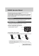
Video Cassette Recorder

PV-V4524S / PV-V4624S / PV-V464S / PV-V4524S-K / PV-454S-K / 

PV-V4624S-K

For servicing the R4-Mechanism Chassis for PV-Model, Please refer to 
the R4-Mechanism Chassis for PV-Model Service Manual (Order No. 
MKE0401000C1). 

SPECIFICATIONS

   2004 Matsushita Kotobuki Electronics Industries Ltd. All rights 
reserved. Unauthorized copying and distribution is a violation of law. 

1

Summary of Contents for PV-V4524S

Page 1: ...V4624S K For servicing the R4 Mechanism Chassis for PV Model Please refer to the R4 Mechanism Chassis for PV Model Service Manual Order No MKE0401000C1 SPECIFICATIONS 2004 Matsushita Kotobuki Electro...

Page 2: ...g as this protects the technician from accidents resulting in personalinjury from electrical shocks It will also protect VCR from being damaged by accidental shorting that may occur during servicing 3...

Page 3: ...own in figure 1 3 Use an AC voltmeter with 1 k V or more sensitivity to measure the potential across the resistor 4 Check each exposed metallic part and measure the voltage at each point 5 Reverse the...

Page 4: ...tatic solder removal device Some solder removal devices not classified as antistatic ESD protected can generate electrical charge sufficient to damage ES devices 5 Do not use freon propelled chemicals...

Page 5: ...ith temperature control and adjust it to 700 F 20 F 370 C 10 C In case of using high temperature soldering iron please be carefull not to heat too long Pb free solder will tend to splash when heated t...

Page 6: ...off condition Fig 1 1 2 Fault code 4 digit number will be displayed in F I P as shown Fig 1 2 4 1 1 Explanation of I 2 C bus transmission number The condition of I2C bus transmission befor shut off i...

Page 7: ...Fig 1 4 4 1 3 Explanation of Error code number The detecting condition and movement of mechanism is displayed Fig 1 5 7...

Page 8: ...4 1 3 1 Reason of Ejection When an error code is 80 the reason of ejection is displayed on the Light Emitting Diode LED display of TIMER VCR and HiFi Fig 1 6 Fig 1 7 8...

Page 9: ...e in hours 1 With power turned on and no cassette press CH DOWN button on VCR and 7 key on remote controller together The USAGE SCREEN will be displayed on the TV Monitor Fig 2 Note 1 After replacing...

Page 10: ...or PV Model Order No MKE0401000C1 4 2 3 SERVICE POSITION 4 2 3 1 Service Position CAUTION HOT CIRCUIT Primary circuit exists on the Main C B A Use extreme care to prevent accidental shock when servici...

Page 11: ...tified as HOT on the C B A and in the Service Manual Use extreme care to prevent accidental shock when servicing 4 2 5 TRACKING CENTER MODE TRACKING FIX AT CENTER Insert the Cassette tape Set the unit...

Page 12: ...ould always be used during the servicing of VCR whose chassis is not isolated from the AC power line Use a transformer of adequate power rating as this protects the technician from accidents resulting...

Page 13: ...to Item 3 of Schematic Diagram Notes of Schematic Diagram Notes for mark PT 5 DISASSEMBLY ASSEMBLY PROCEDURES 5 1 CABINET SECTION 5 1 1 Disassembly Method NOTE When reassembling use the reverse steps...

Page 14: ...5 1 1 1 Notes in chart 1 Installation of Top Cover Install the Top Cover front portion at a downward angle so that the tab on the Front Panel Ass y fits into the hole in the Top Cover Then lower the r...

Page 15: ...y swing the Cassette Door Lid all the way open until the Cassette Door tab clears the Opener Lever 2 Make sure that all locking tabs are aligned properly Then press the Front Panel straight in Fig D1...

Page 16: ...nsor LED clears the hole in the Mechanism Chassis and that 3 Connectors P3501 P4001 P6201 are aligned and seated securely 5 2 MECHANISM SECTION Refer to the Service Manual for R4 Mechanism Chassis for...

Page 17: ...6 5 SIGNAL WAVEFORMS 7 CIRCUIT BOARD LAYOUT 7 1 MAIN C B A 8 BLOCK DIAGRAMS 8 1 OVERALL BLOCK DIAGRAM 9 EXPLODED VIEWS 9 1 MECHANISM SECTION 17...

Page 18: ...9 2 CHASSIS FRAME AND CASING PARTS SECTION 18...

Page 19: ...9 3 PACKING PARTS AND ACCESSORIES SECTION 19...

Page 20: ...T PARTS LISTS BEFORE REPLACING PARTS READ THE FOLLOWING 10 1 REPLACEMENT NOTES 10 1 1 General Notes 1 Use only original replacement parts To maintain original function and reliability of repaired unit...

Page 21: ...service replacement parts 6 Definition of Parts supplier A Parts with mark MKE in the Remarks column are supplied from MKE B Parts without mark in the Remarks column are supplied from MKI 7 Item numbe...

Page 22: ...NR Non Repairable Board Ass y MGF CHIP Metal Glaze Film Chip C CHIP Ceramic Chip COMPLX CMP Complex Component W FLMPRF Wirewound Flameproof C B A Circuit Board Assembly P C B Printed Circuit Board E...

Page 23: ...R UNIT 1 7 VXL3107 SUPPLY LOADING ARM UNIT 1 8 VXL3108 TAKE UP LOADING ARM UNIT 1 9 VEM0796 LOADING MOTOR UNIT 1 10 VXL3110 P5 ARM UNIT 1 11 VXL3112 SUPPLY BRAKE ARM UNIT 1 12 VXL3121 T BRAKE ARM UNIT...

Page 24: ...GP0382 REAR PANEL 2 76 LSKA0012 RUBBER FOOT 2 100 EUR77EC2406A BATTERY COVER A C D E 3 100 EUR77EC0903B BATTERY COVER B F 3 121 LSPG1631 PACKING CASE PAPER A 3 121 LSPG1655 PACKING CASE PAPER B 3 121...

Page 25: ...AC 120V 2 741 LSJA0358 AC CORD W PLUG AC 120V 2 741 LSJA0359 AC CORD W PLUG AC 120V 2 741 LSJA0361 AC CORD W PLUG AC 120V 2 743 ENG56D01G1F TUNER UHF VHF NR A B C 2 743 J3AAADB00001 TUNER UHF VHF NR...

Page 26: ...art No Part Name Description Remarks E10 LSEP2131HA MAIN C B A A E S D RTL E10 LSEP2131HB MAIN C B A B C E S D RTL E10 LSEP2131HD MAIN C B A D E S D RTL E10 LSEP2131HF MAIN C B A E E S D RTL E10 LSEP2...

Page 27: ...Q1203 B1ABGC000003 TRANSISTOR SI NPN CHIP Q1204 2SD0601AHL TRANSISTOR SI NPN CHIP Q1204 B1ABCF000011 TRANSISTOR SI NPN CHIP Q1205 B1BACC000010 TRANSISTOR SI NPN Q1205 2SD1581 T TRANSISTOR SI NPN Q120...

Page 28: ...L TRANSISTOR SI NPN CHIP Q4101 2SD0601ARL TRANSISTOR SI NPN CHIP Q4172 UNR221100L TRANSISTOR SI NPN CHIP Q4172 DTC114EK TX TRANSISTOR SI NPN CHIP Q6001 2SD0601A0L TRANSISTOR SI NPN CHIP Q6001 B1ABCF00...

Page 29: ...DE SI D1013 B0HAJP000007 DIODE SI D1013 B0HAMP000061 DIODE SI D1013 B0HAMP000069 DIODE SI D1201 MAZ4047NMF DIODE ZENER 4 7V D1202 B0AAML000001 DIODE SI D1202 B0EAKL000008 DIODE SI D1204 B0AAML000001 D...

Page 30: ...GEYJ101V MGF CHIP 1 10W 100 R1006 ERJ6GEYJ104V MGF CHIP 1 10W 100K R1007 ERDS2TJ105T CARBON 1 4W 1M R1008 ERDS2TJ105T CARBON 1 4W 1M R1009 ERG2SJ331H METAL OXIDE 2W 330 R1010 ERDS2TJ272 CARBON 1 4W 2...

Page 31: ...GEY0R00V MGF CHIP 1 16W 0 R3032 ERJ3GEYJ685V MGF CHIP 1 16W 6 8M R3033 ERJ3GEY0R00V MGF CHIP 1 16W 0 R3037 ERJ3GEYJ181V MGF CHIP 1 16W 180 R3039 ERDS2TJ680T CARBON 1 4W 68 R3041 ERJ3GEY0R00V MGF CHIP...

Page 32: ...32...

Page 33: ...4 7K R6006 ERDS2TJ151T CARBON 1 4W 150 R6007 ERJ3GEYJ223V MGF CHIP 1 16W 22K R6008 ERJ3GEYJ183V MGF CHIP 1 16W 18K R6009 ERJ3GEYJ391V MGF CHIP 1 16W 390 R6010 ERJ3GEYJ103V MGF CHIP 1 16W 10K R6011 ER...

Page 34: ...34...

Page 35: ...MGF CHIP 1 16W 5 6K R6084 ERJ3GEYJ562V MGF CHIP 1 16W 5 6K R6087 ERJ3GEYJ562V MGF CHIP 1 16W 5 6K R6090 ERJ3GEYJ103V MGF CHIP 1 16W 10K R6091 ERJ3EKF1002V MGF CHIP1 16W 10K R6092 ERJ3GEYJ102V MGF CHI...

Page 36: ...U3D332MX CERAMIC 125V 3300PF C1005 ECEA2DU820YE ELECTROLYTIC 200V 82UF C1005 ORF2A2D8200001 ELECTROLYTIC 220V 82UF C1005 ORF2A2D8200003 ELECTROLYTIC 200V 82UF C1005 ORVCESR2D820XE ELECTROLYTIC 200V 82...

Page 37: ...ECJ1VB1C104K C CHIP 16V 0 1UF C3019 ECJ1VB1C104K C CHIP 16V 0 1UF C3020 ECEA1HKA3R3 ELECTROLYTIC 50V 3 3UF C3021 ECEA1CKA100 ELECTROLYTIC 16V 10UF C3022 ECJ1VB1E103K C CHIP 25V 0 01UF C3025 ECJ1VC1H3...

Page 38: ...38...

Page 39: ...0 ELECTROLYTIC 16V 10UF C4207 ECEA1CKA100 ELECTROLYTIC 16V 10UF C4208 ECEA1CKA100 ELECTROLYTIC 16V 10UF C4209 ECEA1CKA100 ELECTROLYTIC 16V 10UF C4210 ECEA1CKA100 ELECTROLYTIC 16V 10UF C4211 ECJ1VB1H15...

Page 40: ...40...

Page 41: ...J C CHIP 50V 82PF C6033 ECJ1VF1H104Z C CHIP 50V 0 1UF C6034 ECEA0JKA101 ELECTROLYTIC 6 3V 100UF C6035 ECJ1VF1A105Z C CHIP 10V 1UF C6038 ECJ1VB1H102K C CHIP 50V 1000PF C6039 ECJ1VB1H333K C CHIP 50V 0 0...

Page 42: ...L1001 ELF15N005A LINE FILTER 0 5A 18MH L1001 J0HBLD000001 LINE FILTER 0 5A 18MH L1003 J1ZZA0000001 RESONANT SNUBBER L1005 VLQSAB7D100K COIL 10UH L1006 G0A220G00018 COIL 22UH L3001 G0C271JA0019 COIL 2...

Page 43: ...SWITCH SW6306 EVQ11A09K PUSH SWITCH B C F SW6310 EVQ11A09K PUSH SWITCH A D E SW6311 EVQ11A09K PUSH SWITCH SW6314 EVQ11A09K PUSH SWITCH SW6315 EVQ11A09K PUSH SWITCH SW6317 EVQ11A09K PUSH SWITCH SW6320...

Page 44: ...0 AC CORD W PLUG AC 120V 741 LSJA0348 AC CORD W PLUG AC 120V 741 LSJA0358 AC CORD W PLUG AC 120V 741 LSJA0359 AC CORD W PLUG AC 120V 741 LSJA0361 AC CORD W PLUG AC 120V 743 ENG56D01G1F TUNER UHF VHF N...

Page 45: ...tage of Zener Diodes are indicated as such on Schematic Diagrams Example 6 2V Zener Voltage 2 How to identify Connectors Each connector is labeled with a Connector No and Pin No Indicating what it is...

Page 46: ...DIO IN 1 R CH VIDEO IN 2 AUDIO IN 2 L CH AUDIO IN 2 R CH P3502 GND 1 Pins TO MECHANISM CHASSIS IMPORTANT SAFETY NOTICE COMPONENTS IDENTIFIED BY THE SIGN HAVE SPECIAL CHARACTERISTICS IMPORTANT FOR SAFE...

Page 47: ...35 36 37 38 39 40 41 42 43 44 45 46 47 48 49 50 51 52 53 54 55 56 57 58 59 60 61 62 63 64 65 66 67 68 69 70 71 72 73 74 75 81 82 83 84 85 86 87 88 89 90 91 92 93 94 95 96 97 98 99 100 26 27 28 29 30 7...

Page 48: ...0V C3027 47 6 3V C3032 47 6 3V 4R7 25V C3042 3R3 50V C3036 2R2 50V C3037 C3050 47 16V C3051 470 6 3V 330 6 3V C7001 22 16V C4106 J3001 0 PT J3009 J4151 PT J4001 PT J4152 WA17 5 PT J4202 J3008 WA20 J41...

Page 49: ...1 EVQ11A09K SW6312 PT SW6301 PT SW6315 EVQ11A09K SW6316 PT SW6317 EVQ11A09K SW6319 PT SW6318 PT SW6320 EVQ11A09K SW6303 SW6302 GND VCC SW6312 A D E SW6306 CH_UP SW6309 SW6301 SW6315 SW6311 SW6307 POWE...

Page 50: ...B C D F PT D4206 MA165 D4208 MA165 PT R4232 PT R4233 PT C4234 10K R4234 10K R4235 IC4201 AN3663FBP 1 2 3 4 5 6 7 8 9 10 11 12 13 14 15 16 17 18 19 20 21 22 23 24 25 26 27 28 29 30 31 32 33 34 35 36 37...

Page 51: ...6V C1202 0 47 50V C1203 10 16V C1219 10 16V C1221 10 16V C1220 0 47 50V T1001 WF29 LSTP0126 2 4 5 6 15 13 10 14 12 11 9 3 7 16 3300P C1004 0 1 C1003 PT C1001 22U L1006 10U L1005 CNC1S101R1KT IC1001 2...

Page 52: ...B Q4061 IC3001 IC4201 C E B TP6802 TP6036 TP6026 TP1007 TP1002 Q1215 C E B Q1216 C E B J1006 J1007 J1003 TP1205 C1210 TP1003 TP1201 TP1005 TP6304 TP1204 TP6306 TP6305 TP6303 TP1203 Q1207 C E B Q1202 C...

Page 53: ...AUDIO OUT L CH AUDIO OUT R CH RESET Q6003 Q6006 RESET L POWER DOWN L IC6005 RESET 5V TAKEUP REEL SENSOR TAKEUP REEL SENSOR IC6002 SUPPLY REEL SENSOR SUPPLY REEL SENSOR IC6003 TAKEUP PHOTO TR L TAKEUP...

Page 54: ...3 6 50 3 5 51 5 0 52 3 5 53 6 0 54 2 5 MODE STOP PINNO 55 0 56 0 57 6 0 58 12 1 59 6 0 60 0 8 61 2 5 62 2 4 63 2 6 64 0 6 Q1001 S 0 G 1 3 D 22 1 Q1002 E 0 C 1 3 B 0 Q1003 E 0 C 1 3 B 0 4 Q1201 E 29 5...

Page 55: ...4 2 4 15 2 5 2 5 16 2 5 2 5 17 2 5 2 5 18 1 3 1 3 19 5 0 5 0 20 3 6 3 6 21 12 3 12 3 22 3 6 3 6 23 3 6 3 6 24 0 0 25 3 5 3 6 26 0 0 27 0 0 Q6001 E 4 5 0 C 11 1 11 8 B 5 2 0 Q6002 E 11 9 11 9 C 11 8 0...

Page 56: ...OF IC3001 0 5V 0 5ms1 REC PB WF13 1 0Vp p V1 PIN 17 OF IC3001 0 5V 20 s1 REC WF14 1 0Vp p V1 PIN 26 OF IC3001 0 5V 20 s1 REC WF15 1 5Vp p V1 PIN 29 OF IC3001 0 5V 20 s1 REC PB WF16 0 3Vp p V1 PIN 36...

Page 57: ...9 OF T1001 20V 5 s1 POWER ON WF29 36Vp p V1 PIN 11 OF T1001 10V 5 s1 POWER ON WF30 14 0Vp p V1 PIN 10 OF T1001 5V 5 s1 POWER ON WF31 14 0Vp p V1 PIN 15 OF T1001 5V 5 s1 POWER ON WF32 20 0Vp p V1 PIN 6...

Page 58: ...1 42 43 44 45 46 47 48 49 50 51 52 53 54 55 56 57 58 59 60 61 62 63 64 65 66 67 68 69 70 71 72 73 74 75 81 82 83 84 85 86 87 88 89 90 91 92 93 94 95 96 97 98 99 100 26 27 28 29 30 76 77 78 79 80 150 R...

Page 59: ...1 42 43 44 45 46 47 48 49 50 51 52 53 54 55 56 57 58 59 60 61 62 63 64 65 66 67 68 69 70 71 72 73 74 75 81 82 83 84 85 86 87 88 89 90 91 92 93 94 95 96 97 98 99 100 26 27 28 29 30 76 77 78 79 80 150 R...

Page 60: ...7 25V C3042 3R3 50V C3036 2R2 50V C3037 C3050 47 16V C3051 470 6 3V 330 6 3V C7001 22 16V C4106 J3001 0 PT J3009 J4151 PT J4001 PT J4152 WA17 5 PT J4202 J3008 WA20 J4103 PT J4102 PT J4101 PT PT J4002...

Page 61: ...7 25V C3042 3R3 50V C3036 2R2 50V C3037 C3050 47 16V C3051 470 6 3V 330 6 3V C7001 22 16V C4106 J3001 0 PT J3009 J4151 PT J4001 PT J4152 WA17 5 PT J4202 J3008 WA20 J4103 PT J4102 PT J4101 PT PT J4002...

Page 62: ...W6315 EVQ11A09K SW6316 PT SW6317 EVQ11A09K SW6319 PT SW6318 PT SW6320 EVQ11A09K SW6303 SW6302 GND VCC SW6312 A D E SW6306 CH_UP SW6309 SW6301 SW6315 SW6311 SW6307 POWER OUT SW6304 PLAY STOP EJECT SW63...

Page 63: ...W6315 EVQ11A09K SW6316 PT SW6317 EVQ11A09K SW6319 PT SW6318 PT SW6320 EVQ11A09K SW6303 SW6302 GND VCC SW6312 A D E SW6306 CH_UP SW6309 SW6301 SW6315 SW6311 SW6307 POWER OUT SW6304 PLAY STOP EJECT SW63...

Page 64: ...5 PT R4232 PT R4233 PT C4234 10K R4234 10K R4235 IC4201 AN3663FBP 1 2 3 4 5 6 7 8 9 10 11 12 13 14 15 16 17 18 19 20 21 22 23 24 25 26 27 28 29 30 31 32 33 34 35 36 37 38 39 40 41 42 43 44 45 46 47 48...

Page 65: ...5 PT R4232 PT R4233 PT C4234 10K R4234 10K R4235 IC4201 AN3663FBP 1 2 3 4 5 6 7 8 9 10 11 12 13 14 15 16 17 18 19 20 21 22 23 24 25 26 27 28 29 30 31 32 33 34 35 36 37 38 39 40 41 42 43 44 45 46 47 48...

Page 66: ...219 10 16V C1221 10 16V C1220 0 47 50V T1001 WF29 LSTP0126 2 4 5 6 15 13 10 14 12 11 9 3 7 16 3300P C1004 0 1 C1003 PT C1001 22U L1006 10U L1005 CNC1S101R1KT IC1001 2 1 4 3 IC1002 C0DAEMZ00005 2 3 1 F...

Page 67: ...219 10 16V C1221 10 16V C1220 0 47 50V T1001 WF29 LSTP0126 2 4 5 6 15 13 10 14 12 11 9 3 7 16 3300P C1004 0 1 C1003 PT C1001 22U L1006 10U L1005 CNC1S101R1KT IC1001 2 1 4 3 IC1002 C0DAEMZ00005 2 3 1 F...

Page 68: ...VIDEO IN 2 AUDIO IN 2 L CH AUDIO IN 2 R CH P3502 GND 1 Pins TO MECHANISM CHASSIS IMPORTANT SAFETY NOTICE COMPONENTS IDENTIFIED BY THE SIGN HAVE SPECIAL CHARACTERISTICS IMPORTANT FOR SAFETY WHEN REPLAC...

Page 69: ...VIDEO IN 2 AUDIO IN 2 L CH AUDIO IN 2 R CH P3502 GND 1 Pins TO MECHANISM CHASSIS IMPORTANT SAFETY NOTICE COMPONENTS IDENTIFIED BY THE SIGN HAVE SPECIAL CHARACTERISTICS IMPORTANT FOR SAFETY WHEN REPLAC...

Page 70: ...LC YNR PG AGC DET N L DE EMPH SQPB EQ Y LPF TRAP NC HP NC DEH N L EMPH ET LPF PC VIDEO AGC ATT 4dB ATT 10dB ATT 6dB ATT 10dB ATT 10dB 629 TRAP 6dBAMP C K NP CONV B D PILOT ERASE BPF PILOT ADD V AMP SQ...

Page 71: ...LPF PNR LCH AGC GND PREAMP SWITCH VCC REC DC2 HIFI PLAY H NOISE DET PNR RCH BPF BPF LPF FM MODULATOR DEMODULATOR AGC SWITCH MUTE REC AGC ADJ GND VCC FSC MTS MUTE IIC BUS INTERFACE REC AUDIO SIGNAL PB...

Page 72: ...Input terminal of the LC Oscillation For OSD dot clock 45 LC OSC OUT I Output terminal of the LC Oscillation For OSD dot clock 46 NUB Connected to the GND Test terminal B in the factory 47 4FSC LPF I...

Reviews: