background image

Operating temperature

range:

+5 to +35°C (+41 to +95°F)

Operating humidity range:

5-85% RH (no condensation)

Region number:

Region No.3 (DVD-LX110GCS)

Region No.5 (DVD-LX110EE)

Discs played
[8cm (3”) or 12cm (5”)]:

DVD [DVD-Video, DVD-Audio, DivX
(EE only /*6, 8)]

DVD-RAM [DVD-VR, JPEG(*4,6,7),
MP3(*2,6), MPEG4(*5,6), DivX (EE
only /*6, 8)]

DVD-R [DVD-Video, DVD-VR,
JPEG(*4,6,7), MP3(*2,6),
MPEG4(*5,6), DivX (EE only /*6, 8)]

DVD-R DL (DVD-Video, DVD-VR)

DVD-RW [DVD-Video, DVD-
VR,JPEG(*4,6,7), MP3(*2,6),
MPEG4(*5,6), DivX (EE only /*6, 8)]

+R/RW (Video)

+R DL (Video)

CD, CD-R/RW [CD-DA, Video-CD,
SVCD(*1), MP3(*2, 6), WMA(*3, 6),
JPEG (*4,6,7), MPEG4(*5,6), DivX
(EE only /*6, 8), HighMAT Level 2
(Audio and Image)]

©

2006 Matsushita Electric Industrial Co., Ltd. All

rights

reserved.

Unauthorized

copying

and

distribution is a violation of law.

DVD-LX110EE
DVD-LX110GCS

RAE1907Z-C Mechanism Series

Colour
(S).................Silver Type

*1: Conforming to IEC62107

*2: MPEG-1 Layer3, MPEG-2 Layer3

*3: Windows Media Audio Ver9.0 L3.
Not compatible with Multiple Bit Rate
(MBR)

*4: Exif Ver 2.1 JPEG Baseline files
Picture resolution: between 160×120
and 6144×4096 pixels (sub sampling
is 4:0:0, 4:2:2, 4:2:0 or 4:4:4)

*5: MPEG4 data recorded with the
Panasonic SD multi cameras or DVD
recorders Conforming to SD VIDEO
specifications (ASF standard)/MPEG4
(Simple Profile) video system/G.726
audio system.

*6: The total combined maximum
number of recognizalbe audio, picture
and movie contents and groups:
4000 audio, picture and movie
contents and 400 groups.

*7: Extremely long and slender
pictures may not be displayed.

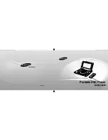
Portable DVD/CD PLAYER

Specifications

ORDER NO.CHM0606037CE

Summary of Contents for DVD-LX110EE

Page 1: ... reserved Unauthorized copying and distribution is a violation of law DVD LX110EE DVD LX110GCS RAE1907Z C Mechanism Series Colour S Silver Type 1 Conforming to IEC62107 2 MPEG 1 Layer3 MPEG 2 Layer3 3 Windows Media Audio Ver9 0 L3 Not compatible with Multiple Bit Rate MBR 4 Exif Ver 2 1 JPEG Baseline files Picture resolution between 160 120 and 6144 4096 pixels sub sampling is 4 0 0 4 2 2 4 2 0 or...

Page 2: ...nt conforming to SD File System specifications Ver 1 01 such as Panasonic SD multi cameras or DVD recorders Conforming to FAT 12 standard and FAT 16 standard 6 miniSDTM card is supported miniSDTM adaptor is required 7 Conforming to SD Picture specifications Picture resolution between 160 120 and 6144 4096 pixels Sub sampling is 4 0 0 4 2 0 4 2 2 or 4 4 4 Headphone output Output Stereo mini jack 3 ...

Page 3: ...INES 7 3 PREVENTION OF ELECTRO STATIC DISCHARGE ESD TO ELECTROSTATICALLY SENSITIVE ES DEVICES 7 4 PRECAUTION OF LASER DIODE 8 5 HOW TO REPLACE THE LITHIUM BATTERY 9 6 Service caution based on legal restrictions 10 6 1 General description about Lead Free Solder PbF 10 This product is licensed under the MPEG 4 Visual patent portfolio license for the personal and noncommercial use of a consumer for i...

Page 4: ...2 POWER SUPPLY BLOCK DIAGRAM 46 14 3 SERVO BLOCK DIAGRAM 47 14 4 VIDEO BLOCK DIAGRAM 48 14 5 AUDIO BLOCK DIAGRAM 49 14 6 LCD DRIVE BLOCK DIAGRAM 51 15 INTERCONNECTION SCHEMATIC DIAGRAM SCHEMATIC DIAGRAM NOTES 53 15 1 INTERCONNECTION SCHEMATIC DIAGRAM 53 15 2 SCHEMATIC DIAGRAM NOTES 54 16 SCHEMATIC DIAGRAM 55 16 1 POWER SUPPLY CHARGE BATTERY SECTION MAIN P C B 1 4 SCHEMATIC DIAGRAM 55 16 2 OPTICAL ...

Page 5: ...r EEPROM Service part 2 Make a photocopy section 1 3 Manual for customer on this service manual Manual for customer has important information for DivX Video on Demand Service user Please don t forget take it to the customer with unit 1 2 About DivX 1 2 1 DivX A video compression format developed by DivXNetworks Inc that compresses video files without any considerable loss of video quality 1 2 2 Ab...

Page 6: ...gistration code otherwise you will no longer be able to play DivX Video on Demand content 3 Follow the procedure on the DivX Video on Demand web site to register at http vod divx com If you do not use the DivX Video on Demand content please ignore this warning Warning for Customers Who Use the DivX Video on Demand content 6 DVD LX110EE DVD LX110GCS ...

Page 7: ...stomer from being exposed to shock hazards 3 PREVENTION OF ELECTRO STATIC DISCHARGE ESD TO ELECTROSTATICALLY SENSITIVE ES DEVICES Some semiconductor solid state devices can be damaged easily by static electricity Such components commonly are called Electrostatically Sensitive ES Devices Examples of typical ES devices are integrated circuits and some field effect transistors and semiconductor chip ...

Page 8: ... ES devices Otherwise hamless motion such as the brushing together of your clothes fabric or the lifting of your foot from a carpeted floor can generate static electricity ESD sufficient to damage an ES device 4 PRECAUTION OF LASER DIODE 8 DVD LX110EE DVD LX110GCS ...

Page 9: ...t must therefore only be fitted in equipment designed specifically for its use Replacement batteries must be of the same type and manufacture They must be fitted in the same manner and location as the original battery with the correct polarity contacts observed Do not attempt to re charge the old battery or re use it for any other purpose It should be disposed of in waste products destined for bur...

Page 10: ...er PbF The lead free solder has to be used when repairing the equipment for which the lead free solder is used Definition The letter of PbF is printed on the PCB using the lead free solder To put lead free solder it should be well molten and mixed with the original lead free solder Remove the remaining lead free solder on the PCB cleanly for soldering of the new IC Since the melting point of the l...

Page 11: ... the job in as short times as possible 3 Be careful not to apply excessive stress to the flexible board FPC Board 4 Do not turn the variable resistor Laser power adjustment 1 Human body grounding Use the antistatic wrist strap to discharge the static electricity from your body 2 Work table grounding Put a conductive material sheet or steel sheet on the area where the optical pickup is placed and g...

Page 12: ...8 DISASSEMBLY REASSEMBLY AND SERVICE POSITION 12 DVD LX110EE DVD LX110GCS ...

Page 13: ...8 1 Disassembly 13 DVD LX110EE DVD LX110GCS ...

Page 14: ...8 2 P C B location 14 DVD LX110EE DVD LX110GCS ...

Page 15: ...emoving battery pack Release the lock lever and remove the battery pack in the direction of the arrow 1 Remove the 16 screws from the bottom of the unit 2 Release the latches and remove the bottom cabinet 15 DVD LX110EE DVD LX110GCS ...

Page 16: ...rse assembly 1 Reinstall the traverse assembly to the specified pin of the unit 2 Reinstall the flexible cable of the optical pickpup unit and lock it securely 3 Remove the solder of each laser short land of the flexible cable Caution Remove the solders completely otherwise the laser diode won t emit light 4 Reinstall the spindle flexible cable as shown figure 16 DVD LX110EE DVD LX110GCS ...

Page 17: ... make sure to remove the solder from each of the two laser short lands on the flexible cable Caution Remove the solders completely otherwise the laser diode won t emit light After replacing the optical pick up unit check the quality of images played back and make optical adjustment 8 6 Disc motor 8 6 1 Removing disc motor 1 Remove the adjustment screws A B and C 2 Remove the disc motor 8 6 2 Cauti...

Page 18: ...s 8 8 Front SW P C B 1 Remove the connector 2 Remove the 4 screws and remove the front SW P C B and IR P C B 8 9 SD card P C B 1 Remove the connector 2 Remove the 3 screws and remove the SD card P C B 8 10 Side SW P C B 1 Remove the connector 2 Remove the 2 screws and remove the side SW P C B 18 DVD LX110EE DVD LX110GCS ...

Page 19: ...e the latches and remove the hinge cover 2 Remove the monitor assembly Caution to be taken when installing monitor assembly 1 Install the hinge shaft holder on the cabinet as shown figure 8 12 Disc cover 1 Remove the screw and remove the hinge angle 19 DVD LX110EE DVD LX110GCS ...

Page 20: ...ver 4 Remove the stopper piece into the direction of the arrow 5 Remove the shaft into the direction of the arrow Caution Please don t lose the spring 8 13 Monitor cover 1 Remove the 8 screws 2 Remove the monitor cover into the direction of the arrow 3 Remove the 2 connectors 20 DVD LX110EE DVD LX110GCS ...

Page 21: ...e mono arm assembly 3 Release the latches and remove the shaft covers 4 Remove the 8 screws 5 Remove the mono arm cover Caution Please don t lose the spring Caution to be taken when installing mono arm 1 Install the monitor cable in the mono arm as shown figure 21 DVD LX110EE DVD LX110GCS ...

Page 22: ... the arrow Caution to be taken when installing LCD I F P C B 1 Reinstall the flexible cables as shown figure 8 16 LCD panel and inverter unit 1 Remove the LCD panel and inverter unit into the direction of the arrow 8 17 Replacing the fuse in the car dc adaptor Replace only with the specified 125V 250V 3A fuse Use of any other type can cause fire 22 DVD LX110EE DVD LX110GCS ...

Page 23: ...the rubber cushion from the traverse assembly to prevent it from getting damaged 3 Install a dick on the traverse assembly Caution Make sure the disk is securely installed on the disk motor 4 Remove the main P C B operation P C B inverter P C B and LCD panel as shown below 5 The disk cannot be played back with the disk cover removed Press and hold down the S5201 and S5202 Secure with cellulose tap...

Page 24: ...efficiently determine the problem and adjust tilt If NO DISC is displayed before exchanging the optical pick up carry out problem diagnosis first If the present laser driving current is over 55 the optical pick up may need to be exchanged Note Carry out diagnosis within 3 minutes of turning the unit on The player s current can increase as it warms up so turn the unit off and allow it to cool down ...

Page 25: ...ckup Note When using a soldering iron which is not destaticized short circuit the terminal face of the flexible case with a clip After that short circuit the land After the repairing work is completed remove the solder according to the correct procedure shown in this Technical Guide 9 2 UHF displays Use the internal service mode for evaluation of malfunctions Display Method Display Diagnosis Items...

Page 26: ...ervo error H04 Tracking servo error H05 Seek error H06 Power error Cannot switch off the power because of the panel and system computer communication error H07 Spindle motor drive error DSC related F500 DSC error DSC stops in the occurence of servo error starup focus error etc OPU DV3 2 IC3004 DV3 2 IC3004 servo drive F501 DSC not Ready DSC system computer communication error Communication failure...

Page 27: ...age command changes Message is changed before it is sent as a reply to disc manager F880 Task number is not appropriate Message coming from a non existing task F890 Sending message when message is being sent to AV task Sending message to AV task F891 Message couldn t be sent to AV task Begin sending message to AV task F893 FROM falsification FROM IC3001 DV3 2 IC3004 F894 EEPROM abnormality EEPROM ...

Page 28: ...ited by the restricted region code F0C2 A DVD PAL restricted playback F0C3 B DVD Parental lock setting prohibits the playback of the entire title F0C4 C VCD Prohibited because it is in PHOTO CD fromat F0C5 VCD CD Prohibited because it is CDROM without CD DA 9 6 Service mode table Pressing various button combinations on the player and remote control unit can activate the service modes 28 DVD LX110E...

Page 29: ...29 DVD LX110EE DVD LX110GCS ...

Page 30: ...9 7 Lens cleaning When cleaning the lens use the lens cleaner which product part No SZZP1038C 30 DVD LX110EE DVD LX110GCS ...

Page 31: ...r may be renewed to improve the quality including operationability and playerbility to the substandard discs processing to optimize the drive The recovery disc has also firmware version up After version up recovery processing is executed automatically Part number of the recovery disc for version up will be noticed when it is supplied Updating firmware 1 Load the recovery disc that is supplied to t...

Page 32: ...ical pickup peripheral parts such as rail Notes Adjustment is generally unnecessary after replacing other parts of the traverse unit However make adjustment if there is a noticeable degradation in picture quality Optical adjustments cannot be made inside the optical pickup 11 2 2 Important points in electrical adjustment Follow the adjustment procedures described in this Manual 11 3 Storing and Ha...

Page 33: ...make the adjustment 11 4 1 1 Preparations 1 Connect the main P C B to the traverse ass y with the extension cable 2 Install the traverse ass y to the tilt adjustment jig with three screws and three washers Caution Remove the rubber cushion of the traverse ass y 3 Install the traverse ass y to the disc Caution Make sure the disc is installed on the disc motor securely 4 Disassemble the Main P C B O...

Page 34: ...ze the jitter value in the tangential direction Once turn the screw to the full position and then back off You should finish tightening in the tightening direction 5 DISC height measurement Measure the middle of the deflection of the disc and motor surface If the measured height is out of range adjust to the specified value using the adjustment screws A B and C by the same angle 11 4 1 3 Checking ...

Page 35: ...ontrol unit DVD player remote control Details of adjustment Input video signal Press and buttons on remote controller set the right side number to 71 11 5 2 Adjusting DC offset of impressed voltage Adjustment is required when Check point Noise such as horizontal stripes is found on the screen TL8401 Adjustment procedure Adjustment UP Adjustment DOWN Use 3 on remote control unit DVD player remote c...

Page 36: ...chrome 11 5 8 Adjusting TINT Adjustment is required when Check point TL8604 Adjustment procedure Adjustment UP Adjustment DOWN Use 5 on remote control unit DVD player remote control unit DVD player remote control Details of adjustment Input video signal Press and buttons on remote controller set the number of center to 75 75 color bar 11 5 9 Adjusting color Adjustment is required when Check point ...

Page 37: ...ATA RESPONSE DIGITAL SERVO CONTROLLER DATA SLICE LOOP FILTER DIGITAL VIDEO DISC INITIAL LOGO ABBREVIATIONS E EC ECR ENCSEL ETMCLK ETSCLK ERROR TORQUE CONTROL ERROR TORQUE CONTROL REFERENCE ENCODER SELECT EXTERNAL M CLOCK 81MHz 40 5MHz EXTERNAL S CLOCK 54MHz F FBAL FCLK FE FFI FEO FG FSC FSCK FOCUS BALANCE FRAME CLOCK FOCUS ERROR FOCUS ERROR AMP INVERTED INPUT FOCUS ERROR AMP OUTPUT FREQUENCY GENER...

Page 38: ...ATA VALIDITY SUB CODE SERIAL SUB CODE CLOCK SUB CODE Q DATA SYSTEM CLOCK T TE TIBAL TID TIN TIP TIS TPSN TPSO TPSP TRCRS TRON TRSON TRACKING ERROR BALANCE CONTROL BALANCE OUTPUT 1 BALANCE INPUT BALANCE INPUT BALANCE OUTPUT 2 OP AMP INPUT OP AMP OUTPUT OP AMP INVERTED INPUT TRACK CROSS SIGNAL TRACKING ON TRAVERSE SERVO ON INITIAL LOGO ABBREVIATIONS V VBLANK VCC VCDCONT VDD VFB VREF VSS V BLANKING C...

Page 39: ...f No MODE 1 2 3 4 5 1 2 3 4 PLAY 11 3 0 3 3 9 9 11 0 3 3 8 9 0 1 0 STOP 11 1 0 3 3 8 9 10 8 3 3 9 0 0 0 Ref No MODE 1 2 3 4 5 6 7 8 9 10 11 12 13 14 15 16 PLAY 1 3 0 9 5 0 9 3 4 5 0 3 1 0 1 0 0 5 0 9 4 5 0 3 5 6 5 6 0 8 9 STOP 1 3 0 9 5 0 9 3 4 5 0 2 1 0 1 0 0 7 0 7 4 5 0 2 5 4 5 3 0 8 9 Ref No MODE 1 2 3 4 5 6 7 8 9 10 11 12 13 14 15 16 17 18 19 20 PLAY 1 6 1 6 1 5 1 6 1 6 1 6 0 5 4 3 2 0 3 1 2 4...

Page 40: ...97 198 199 200 PLAY 0 0 0 3 2 0 0 3 2 3 2 0 0 0 0 0 0 0 0 3 2 2 0 2 4 2 7 STOP 0 0 0 3 2 0 0 3 2 3 2 0 0 0 0 0 0 0 0 3 2 2 9 2 7 2 8 Ref No MODE 201 202 203 204 205 206 207 208 209 210 211 212 213 214 215 216 217 218 219 220 PLAY 2 5 2 6 2 5 3 2 0 2 6 2 3 2 4 2 3 2 4 2 3 2 4 2 6 3 2 0 2 4 2 4 1 0 1 9 1 9 STOP 3 0 2 9 3 2 3 2 0 3 0 2 9 2 9 3 1 2 9 3 0 3 2 2 9 3 2 0 2 7 2 8 1 1 2 6 2 6 Ref No MODE 2...

Page 41: ...0 0 Ref No MODE 21 22 23 24 25 26 27 28 29 30 31 32 33 34 35 36 37 38 39 40 PLAY 0 0 1 0 1 0 0 3 0 7 3 3 3 3 0 0 3 2 3 3 3 3 2 9 0 0 0 0 3 0 2 6 STOP 0 0 0 0 0 2 0 7 3 3 3 3 0 0 3 2 3 3 3 3 2 9 0 0 0 0 3 0 2 7 Ref No MODE 41 42 43 44 45 46 47 48 49 50 51 52 53 54 55 56 57 58 59 60 PLAY 2 9 3 3 3 3 3 3 0 1 3 3 2 7 3 3 3 3 0 0 3 3 3 3 0 3 3 3 3 0 4 0 0 0 STOP 2 9 3 3 3 3 3 3 0 1 3 3 2 7 3 3 3 3 0 0 ...

Page 42: ...1 3 0 3 2 0 1 3 1 0 0 1 3 1 STOP 0 0 6 0 0 0 6 0 3 2 0 1 3 1 0 0 1 3 1 Ref No MODE E C B E C B E C B E C B E C B PLAY 0 1 0 0 0 2 8 0 0 2 8 0 0 2 2 0 0 0 2 7 STOP 0 0 6 0 0 0 0 0 0 4 5 0 2 0 0 0 0 2 7 Ref No MODE 1 2 3 4 5 6 1 2 3 4 5 6 E C B PLAY 0 1 3 0 0 5 2 0 0 1 6 0 0 5 2 0 3 2 3 2 0 1 STOP 0 0 7 0 0 0 7 0 0 0 7 0 0 0 7 0 3 2 0 1 3 2 Ref No MODE E C B E C B E C B PLAY 0 0 1 3 3 0 3 3 0 0 3 3 ...

Page 43: ... 180 PLAY 0 1 0 6 0 1 0 1 1 1 0 7 0 1 0 5 0 6 0 6 0 6 0 1 0 1 0 1 1 2 0 3 0 1 0 1 0 1 STOP 0 1 0 5 0 1 0 1 0 1 0 5 0 1 0 4 0 5 0 7 0 6 0 1 0 1 0 1 1 4 0 3 0 1 0 1 0 1 Ref No MODE 181 182 183 184 185 186 187 188 189 190 191 192 193 194 195 196 197 198 199 200 PLAY 2 9 0 9 0 2 0 2 0 1 1 5 2 9 2 8 0 1 0 1 0 1 0 1 0 1 0 1 0 1 0 1 0 1 0 1 0 1 0 1 STOP 2 9 1 0 0 1 0 2 0 1 1 5 2 9 2 8 0 1 0 1 0 1 0 1 0 1...

Page 44: ... 3 7 2 0 2 0 1 5 0 1 2 0 1 5 2 0 4 9 Ref No MODE 1 2 3 4 5 6 7 8 9 10 11 12 13 14 15 16 PLAY 2 5 0 1 3 2 2 1 4 9 4 7 4 9 1 9 2 0 0 1 3 1 3 1 1 0 1 1 1 7 1 8 STOP 2 4 0 1 3 2 2 1 4 9 4 7 4 9 1 9 2 0 0 1 3 1 3 1 1 0 1 1 1 7 1 8 Ref No MODE E C B E C B E C B E C B E C B PLAY 1 5 0 1 8 0 9 3 0 1 5 1 5 0 1 8 0 9 3 0 1 5 0 3 0 9 3 0 STOP 1 5 0 1 8 0 9 3 0 1 5 1 5 0 1 8 0 9 3 0 1 5 0 3 3 0 0 9 Ref No MOD...

Page 45: ... FLASH 32Mbit 8Kbit IC6002 IC2601 IC2651 MECHANISM UNIT TRAVERSE MAIN P C B COIL TRACKING COIL FOCUS MPU OPERATION KEY CONTROL REMOTE LED SELECTOR DRIVE MOTOR TRAVERSE MOTOR TRAVERSE DRIVE MOTOR SPINDLE MOTOR SPINDLE UNIT PICK UP OPT OUT IC4008 IC4004 SELECTOR IC3203 HEADPHONE AUDIO IN OUT LCD IC3009 VIDEO IN OUT IC8002 IC3201 IC4003 DRIVE VIDEO CONTROLLER LCD CONVERTER D A AUDIO AUDIO POWER AMP D...

Page 46: ...1402 CTL QR1403 JK1401 JW1401 1 FP6201 3 FP6811 3 FP6201 2 FP6811 4 FP6210 1 FP6801 1 FP6201 1 FP6811 5 QR6003 LED DRIVE FP6210 4 FP6801 4 FP6210 3 FP6801 3 FP6210 2 FP6801 2 1 IP1401 IP1421 DC IN BAT JK1401 DC IN JW1401 BATTERY ADP ON IC6002 SIDE SW P C B OPERATION MPU 5 PA3 60 P63 6 PA4 KEY2 KEY1 79 P81 80 P80 59 P62 KEY3 7 PA5 FP6201 4 FP6811 2 D6004 PWR SW DVDON H LCDON H PON H 18 NRST 44 P42 ...

Page 47: ...DRV4 DRV1 FG DRV2 VHALF HFG TRV SW LASER DIODE Q5202 Q5215 LD DRIVE VREFH LPCO1 LPC1 LPCO2 LPC2 VIN4 VIN3 VIN2 PWM1 PWM0 DRV0 DRV3 VIN1 VIN8 VIN7 VIN6 VIN5 OPTICAL PICK UP UNIT PHOTO DETECTOR B3 B4 B2 B1 A3 A2 A4 A1 LASER DIODE DVDLD CDLD AMP HEAD Q5201 Q5211 LD DRIVE 131 DV3 2 IC3004 SPINDLE MOTOR DRIVE SPINDLE MOTOR UNIT IC2651 132 133 134 138 137 135 136 127 124 123 126 125 113 114 128 145 144 ...

Page 48: ...C3004 156 DV3 2 157 IC3004 DAC5OUT EXT MUTE LCD MUTE AVIN INV 156 DAC4OUT 149 DAC1OUT 148 DAC2OUT 147 DAC3OUT CVOUT PY GOUT PB BOUT PR ROUT VIDEO SIGNAL AMP 6MHz LPF 12MHz LPF BIAS CIN YIN PY GIN PB BIN PR RIN PROUT PBOUT PYOUT VYOUT VCOUT FROM IC6002 74pin FROM IC6002 73pin FROM IC6002 75pin BIAS MUTE1 75Ω 6dB 6dB VIDEO DRIVE IC3201 30 29 75Ω 24 23 12MHz LPF 6dB 75Ω 21 20 4 5 MUTE2 14 CLAMP MUTE ...

Page 49: ... OUT 15 17 19 18 24 10 12 21 5 S DOWN 2 7 25 5 15 16 80 64 14 LPF BUFFER QR6001 AVIN INV QR4014 MUTE QR4015 D4004 IC6003 BUFFER D A ZERR ZEROA MANAGER CLOCK SYSTEM MODULATOR CONTROLLER LPF VOUTR VOUTL D A DATA BCK LRCK SCK PORT SERIAL AUDIO 8 7 6 DV3 2 AUDIO DAC IC4003 B 9 A X0 X DVD TUNER 10 12 X3 11 X2 15 Y3 4 Y2 2 Y0 1 13 Y 3 SELECTOR IC4004 INA 2 OUTA 8 OUTB 5 O CNT 4 INB 3 SW AMP IC4006 AUDIO...

Page 50: ... HPJOPEN H JK4703 1 5 4 3 2 HEAD PHONE CSPON H AUDIO SIGNAL BST AGC BOOST BST SW MT SW SW 13 18 MUTE SW 17 HP AMP BST1 PWB PWA INB INA OUTA OUTB AGC IN BST OUT BST2 IC4701 3 4 6 8 12 FROM IC6002 63pin FROM IC6002 62pin POWER MUTE XBSON H P8001 8 P3201 41 P8001 7 P3201 CNT SP TO LCD P C B CNT SP 42 IC4101 SP AMP 1 SHUT DOWN 8 VO2 4 IN 5 VO1 A B C DVD LX110EE DVD LX110GCS 50 ...

Page 51: ... 186 194 190 191 192 100 VCO1 ASWOUT2 AD2AIN DVD LX110EE GCS LCD DRIVE BLOCK DIAGRAM IC8002 91 1 2Vp p 20usec div IC6002 30PIN FROM O STB 5V CS SCK SCL SIN SDA IC6002 55PIN FROM O CLK 5V IC6002 50PIN FROM O DATA 5V IC6002 51PIN FROM I2CDAT IC6002 53PIN FROM I2CCLK IC6002 52PIN FROM IC6002 29PIN FROM IC8903 CLOCK OSCILLATOR 4 3 9 8 AMP1 AMP2 1 2 VCO PD PV AMP 15 16 IC8101 OSD CONTROLLER 22 20 18 17...

Page 52: ...DVD LX110EE DVD LX110GCS 52 ...

Page 53: ...33 32 31 I2CDAT O DATA 5V 11 O STB 5V I2CCLK MIFRST 5V 10 9 8 7 6 AVDD 5 0V 2 1 3 4 VON 13 5V AVDD 5 0V VEE 23 7V P3201 DGND 5 LCD_HON H 12 13 14 15 16 17 18 19 20 21 22 23 24 25 26 27 28 29 30 O CLK 5V DGND MIFCLK MIFSTRB MIFDAT VSYNCMON VMODE2 VMODE1 VDD 3 7V VDD 3 7V DGND PWRGND PWRGND PWRGND PWRGND DGND VGND LCDCV VGND OPR 3R3V 1 1 OPR 3R3V OPR 3R3V EGND 8 OPR 3R3V 8 KEY1 FP6801 DGND PLAY KEY2...

Page 54: ...omponents used in this equipment which are important for safety These parts are marked by in the schematic diagrams It is essential that these critical parts should be replaced with manufacturer s specified parts to prevent shock fire or other hazards Do not modify the original design without permission of manufacturer Caution IC and LSI are sensitive to static electricity Secondary trouble can be...

Page 55: ...TCHING SWITCHING SWITCHING SWITCHING SWITCHING REG 12V REG 3 3V REG 5 5V REG 3 7V REG SWA 5V REG A 5V REG LCD 5V SWITCHING ADP ON L SWITCHING SWITCHING TO JW1402 BATTERY JACK P C B ADAPTOR 11 10 9 8 7 6 5 4 3 2 1 G F E D C B A A P POWER SUPPLY CHARGE BATTERY SECTION A OP OPTICAL PICKUP SERVO OPERATION SECTION D3 DV3 SECTION AV AUDIO OUT VIDEO OUT SECTION B C D DVD LX110EE GCS POWER SUPPLY CHARGE B...

Page 56: ...ESE11MV9T INV INV 47K R6040 47K INV OPERATION MPU VOL AMP RESET IC TRAVERSE MOTOR DRIVE SPINDLE MOTOR DRIVE TO TRAVERSE MECHANISM UNIT RF SIGNAL 11 10 9 8 7 6 5 4 3 2 1 G F E D C B A B P POWER SUPPLY CHARGE BATTERY SECTION A OP OPTICAL PICKUP SERVO OPERATION SECTION D3 DV3 SECTION AV AUDIO OUT VIDEO OUT SECTION B C D DVD LX110EE GCS OPTICAL PICKUP SERVO OPERATION SECTION MAIN P C B 2 4 SCHEMATIC D...

Page 57: ...A0Y320 DV3 2 SDRAM C3ABPG000133 AUDIO SIGNAL VIDEO SIGNAL RF SIGNAL SD SIGNAL 11 10 9 8 7 6 5 4 3 2 1 G F E D C B A C P POWER SUPPLY CHARGE BATTERY SECTION A OP OPTICAL PICKUP SERVO OPERATION SECTION D3 DV3 SECTION AV AUDIO OUT VIDEO OUT SECTION B C D DVD LX110EE GCS DV3 SECTION MAIN P C B 3 4 SCHEMATIC DIAGRAM DVD LX110EE DVD LX110GCS 57 ...

Page 58: ...V MUTE CTL MUTE CTL MUTE CTL MUTE CTL AUDIO POWER AMP AMP AMP TO P8006 P8001 LCD I F P C B HEADPHONE AMP MUTE MUTE AUDIO IN OUT HEADPHONE HEADPHONE VIDEO IN OUT AUDIO SIGNAL VIDEO SIGNAL 11 10 9 8 7 6 5 4 3 2 1 G F E D C B A D P POWER SUPPLY CHARGE BATTERY SECTION A OP OPTICAL PICKUP SERVO OPERATION SECTION D3 DV3 SECTION AV AUDIO OUT VIDEO OUT SECTION B C D DVD LX110EE GCS AUDIO OUT VIDEO OUT SEC...

Page 59: ...000307 R8613 J0JCC0000307 R8614 J0JCC0000307 R8615 J0JCC0000307 R8618 1K R8620 1K R8619 1K 0 1 C8105 0 1 C8103 0 01 C8102 5V PAL 0 1 C8203 C8202 1000P R8935 22K R8934 22K R8933 22K R8932 3300 R8101 100 R8204 220 G1C100K00020 L8201 C0JBAA000175 IC8203 3Y 3A 3B 4Y 4A 4B VCC GND 2Y 2B 2A 1Y 1B 1A 8 9 10 11 12 13 14 7 6 5 4 1 2 3 G1C100K00020 L8101 C1AB00002200 IC8101 HOR VERT VSS1 BIN P1 R P3 G P3 G ...

Page 60: ...GD3 AGND32 AD3AIN NC NC NC AD3RBS AD3VCLMP AD3VRB NC NC AD3VRT AD3VRTS AVDD32 NC AVDD31 DVDD3 GND VDD ASWOUT3 AGND71 ASW3CIN ASW3BIN ASW3AIN AVDD71 BUNR1 TEB GND GND GND 100u L8018 0 R8021 CL8018 CL8016 CL8013 CL8010 CL8017 CL8014 R8018 120 330P C8051 C8050 0 1 100u L8016 CL8008 CL8007 0 R8013 CL8006 C8042 CL8015 6V47 C8043 330 R8012 100 R8066 0 1 C8046 2SD1819A0L Q8005 100u L8012 100u L8011 330P ...

Page 61: ...00101 10K R8906 0 R8902 ERJ3GEY392V R8904 390 R8921 5600P C8914 47P C8923 1000P C8927 0 1 C8919 1000P C8906 J0JBC0000036 L8904 8200P C8918 H0J214500002 X8902 0 R8924 0 R8926 10P C8913 MA3X028TAL D8901 2 1 3 TL8904 3 2 1 F1J1A105A013 FL8901 AN3917S E1V IC8903 G1C100K00020 L8202 SDA SCL WP VCC GND A2 A1 A0 8 7 6 5 4 3 2 1 C3EBGC000056 IC8204 ERJ6GEY0R00V L8501 22K R8503 R8518 22 R8512 10K R8513 10K ...

Page 62: ...R8070 0 R8065 J0JCC0000119 R8063 J0JCC0000119 R8067 0 TL8802 CKE29 TL8801 CKE27 CKE26 CKE25 CKE24 CKE23 CKE22 CKE21 CKE20 CKE19 CKE18 CKE16 CKE15 CKE14 CKE12 CKE11 CKE10 CKE9 CKE8 CKE7 CKE6 CKE5 CKE4 CKE3 CKE2 CKE1 CKD29 CKD28 TL8902 CKD25 CKD24 CKD22 CKD20 CKD19 CKD18 CKD17 CKD16 CKD15 CKD7 CKD1 CKD2 CKD3 CKD4 CKD5 CKD6 CKD8 CKD9 CKD10 CKD13 CKD11 TL8901 CKD12 R8080 22 33P C8063 FP8003 LCD PANEL ...

Page 63: ... 022 1M 0 022 47K G1C100K00020 10V47 C0DBAGZ00016 G1C220KA0038 MAJ11100L B1CFMC000005 SWICHING 47P 100K 12K 3300 10V47 10K 10V10 3300 F1J1A225A003 0 01 0 1 100 100 100 F1J1A225A003 F1J1A225A003 F1J1A225A003 XP0450100L AMP 0 1 AN2546FH AV VIDEO SIGNAL PROCESSOR 0 0 1 0 1 0 1 0 1 0 1 10V22 0 1 0 1 3900 5600 0 1 1 1 1 18P 27P 56P 0 1 SWITCHING UNR221100L SWITCHING MA2SD2400L MA2SD2400L SWITCHING LCD ...

Page 64: ...16 7 SIDE SW SCHEMATIC DIAGRAM TO FP6201 MAIN P C B SERVO OPERATION SECTION 11 10 9 8 7 6 5 4 3 2 1 G F E D C B A DVD LX110EE GCS SIDE SWITCH SCHEMATIC DIAGRAM DVD LX110EE DVD LX110GCS 64 ...

Page 65: ...16 8 FRONT SW SCHEMATIC DIAGRAM TO FP6210 MAIN P C B SERVO OPERATION SECTION 11 10 9 8 7 6 5 4 3 2 1 G F E D C B A DVD LX110EE GCS FRONT SWITCH SCHEMATIC DIAGRAM DVD LX110EE DVD LX110GCS 65 ...

Page 66: ...16 9 SD CARD SCHEMATIC DIAGRAM TO FP3002 MAIN P C B DV3 SECTION SD SIGNAL 11 10 9 8 7 6 5 4 3 2 1 G F E D C B A DVD LX110EE GCS SD CARD SCHEMATIC DIAGRAM DVD LX110EE DVD LX110GCS 66 ...

Page 67: ...TO FP6210 MAIN P C B SERVO OPERATION SECTION 5 4 3 2 1 C B A DVD LX110EE GCS IR SCHEMATIC DIAGRAM TO JW1401 MAIN P C B POWER CHG BAT SECTION TO BATTERY 5 4 3 2 1 C B A DVD LX110EE GCS BATTERY JACK SCHEMATIC DIAGRAM DVD LX110EE DVD LX110GCS 67 ...

Page 68: ...DVD LX110EE DVD LX110GCS 68 ...

Page 69: ...RCUIT BOARD ASSEMBLY 17 1 MAIN P C B 1 2 COMPONENT SIDE 1 A B C D E F 2 3 4 5 6 7 8 9 DVD LX110EE GCS MAIN P C B 1 2 RFKBLX110EET EE RFKBLX110GCS GCS MAIN P C B 1 2 COMPONENT SIDE DVD LX110EE DVD LX110GCS 69 ...

Page 70: ...406 F 6 C CL4004 A 4 C CL6022 D 2 F Q5211 A 5 F IC3002 D 4 C CL1601 E 6 C CL4005 B 2 F CL6023 D 5 C Q5215 B 5 F IC3004 C 5 C CL1602 E 6 C CL4006 C 6 C IC3007 C 4 C CL2651 B 3 C CL4007 C 6 C S5201 E 3 F QR1007 D 6 C IC3009 C 2 F CL2652 B 3 C CL4008 B 6 C S5202 E 3 F QR1008 D 6 C IC3201 B 4 C CL2653 B 4 C CL4009 B 6 C S6005 F 3 F QR1202 D 6 C IC3202 E 4 C CL2654 B 3 C CL4010 B 7 C QR1402 E 6 C IC320...

Page 71: ... 4 Q8801 C 8 IC8301 C 2 CL8002 C 3 CL8014 B 4 CL8027 C 4 TL8001 C 3 TL8202 B 4 P8001 A 2 Q8007 B 1 Q8802 C 8 IC8001 B 7 IC8302 C 2 CL8003 D 3 CL8015 B 4 CL8028 C 4 TL8002 C 4 TL8203 B 4 P8006 A 4 Q8301 C 1 IC8002 C 4 IC8501 B 9 CL8004 B 3 CL8016 B 4 CL8029 B 4 TL8003 B 4 TL8801 B 8 Q8302 C 1 QR8001 B 1 IC8003 B 6 IC8502 B 8 CL8005 D 3 CL8017 B 4 CL8031 B 4 TL8004 C 3 TL8802 B 8 Q8303 C 2 QR8304 C ...

Page 72: ... 1 A B C D E F 2 3 4 5 6 7 8 9 DVD LX110EE GCS BATTERY JACK P C B REP4003BB C SD CARD P C B REP4004BC C IR P C B REP4004BD C SIDE SW P C B REP4004BA C FRONT SW P C B REP4004BB C FRONT SW P C B SIDE SW P C B SD CARD P C B IR P C B BATTERY JACK P C B DVD LX110EE DVD LX110GCS 72 ...

Page 73: ...18 EXPLODED VIEWS 18 1 Casing Parts Mechanism Section Exploded View 73 DVD LX110EE DVD LX110GCS ...

Page 74: ...18 2 Mechanism Section Exploded View 74 DVD LX110EE DVD LX110GCS ...

Page 75: ...18 3 Packing Accessories Exploded View 75 DVD LX110EE DVD LX110GCS ...

Page 76: ...INK PLATE 1 28 XTN17 6GFJK SCREW 8 29 EAS2D10B SPEAKER 1 30 REZ1765 FFC 5P 1 31 REZ1767 FFC 11P 1 32 RMB0863 SD LOCK SPRING 1 Ref No Part No Part Name Description Pcs Remarks 33 RGQ0456 S DISC HINGE COVER 1 34 RGU2478A S MAIN BUTTON L 1 35 RGU2479 S MAIN BUTTON R 1 36 RGU2480 S OPERATION BUTTON 1 37 RGU2482 S DISC OPEN BUTTON 1 38 RGU2483 S SD OPEN BUTTON 1 39 RKM0559A S MAIN CABINET 1 EE 39 RKM05...

Page 77: ...1U 1 Ref No Part No Part Name Description Pcs Remarks C1401 ECJ0EB1C103K 16V 0 01U 1 C1402 ECJ0EC1H101J 50V 100P 1 C1403 ECJ3YB1E105K 25V 1U 1 C1404 F2H1E680A003 25V 68U 1 C1405 ECJ0EF1C104Z 16V 0 1U 1 C1406 ECJ0EC1H101J 50V 100P 1 C1407 F2G1C101A038 16V 100U 1 C1409 F3F0J226A057 6 3V 22U 1 C1410 ECJ0EC1H101J 50V 100P 1 C1411 ECJ3YB1E105K 25V 1U 1 C1412 F3F1C106A042 16V 10U 1 C1413 ECJ3YB1E475K 25...

Page 78: ... C3216 ECJ1VB0J105K 6 3V 1U 1 C3217 ECJ0EF1C104Z 16V 0 1U 1 C3218 ECJ1VB0J105K 6 3V 1U 1 Ref No Part No Part Name Description Pcs Remarks C3219 ECJ1VB0J105K 6 3V 1U 1 C3220 ECJ1VB0J105K 6 3V 1U 1 C3221 F1G1A104A014 10V 0 1U 1 C3223 ECJ0EC1H101J 50V 100P 1 C3224 F1G1A104A014 10V 0 1U 1 C3225 ECJ0EC1H101J 50V 100P 1 C3226 F1G1A104A014 10V 0 1U 1 C3227 ECJ1VB0J105K 6 3V 1U 1 C3228 ECJ1VB0J105K 6 3V 1...

Page 79: ...C8023 ECJ2YB1A684K 16V 0 68U 1 C8024 ECJ2YB1A684K 16V 0 68U 1 C8025 F1G1A104A014 10V 0 1U 1 Ref No Part No Part Name Description Pcs Remarks C8026 F1G1A104A014 10V 0 1U 1 C8027 F1G1A104A014 10V 0 1U 1 C8028 F1G1A104A014 10V 0 1U 1 C8029 ECJ0EB1E331K 25V 330P 1 C8030 ECJ0EB1C103K 16V 0 01U 1 C8031 F1G1A104A014 10V 0 1U 1 C8032 ECJ0EB1E331K 25V 330P 1 C8033 F1G1A104A014 10V 0 1U 1 C8034 ECJ0EB1E331K...

Page 80: ...G1A104A014 10V 0 1U 1 C8802 ECJ0EB1C103K 16V 0 01U 1 C8803 ECJ0EB1C103K 16V 0 01U 1 C8804 ECJ0EB1C103K 16V 0 01U 1 C8805 ECJ0EB1C103K 16V 0 01U 1 C8806 F3F0J476A047 6 3V 47U 1 C8901 ECJ0EB1C103K 16V 0 01U 1 Ref No Part No Part Name Description Pcs Remarks C8902 ECJ2YB1A684K 16V 0 68U 1 C8903 F1G1A104A014 10V 0 1U 1 C8904 ERJ2GE0R00X 1 16W 0 1 C8906 ECJ1VB1H102K 50V 1000P 1 C8908 ECJ1VB0J105K 6 3V ...

Page 81: ...6 C0JBAB000613 IC 1 IC8007 C0ABBA000075 IC 1 Ref No Part No Part Name Description Pcs Remarks IC8008 C0JBAR000423 IC 1 IC8101 C1AB00002200 IC 1 IC8203 C0JBAA000175 IC 1 IC8204 C3EBGC000056 IC 1 IC8301 AN2546FH AV IC 1 IC8302 C0DBAGZ00016 IC 1 IC8501 C0ABCA000038 IC 1 IC8502 C0FBBD000191 IC 1 IC8601 C1AB00001379 IC 1 IC8603 C1AB00000084 IC 1 IC8701 C0DBZGD00038 IC 1 IC8702 C0DBZGD00038 IC 1 IC8801 ...

Page 82: ... J0JHC0000045 COIL 1 LB4001 J0JCC0000101 COIL 1 LB4002 J0JCC0000101 COIL 1 LB4003 J0JBC0000028 COIL 1 LB4004 J0JBC0000028 COIL 1 Ref No Part No Part Name Description Pcs Remarks LB4005 J0JCC0000101 COIL 1 LB4701 J0JBC0000028 COIL 1 LB4702 J0JBC0000028 COIL 1 LB4703 J0JBC0000028 COIL 1 LB4704 J0JBC0000028 COIL 1 LB4706 J0JBC0000028 COIL 1 LB4707 J0JBC0000028 COIL 1 LB4708 J0JBC0000028 COIL 1 LB4709...

Page 83: ... 33K 1 R1014 ERJ2RHD103X 1 16W 10K 1 R1015 ERJ2RHD333X 1 16W 33K 1 Ref No Part No Part Name Description Pcs Remarks R1016 ERJ2GEJ183X 1 16W 18K 1 R1018 ERJ2GEJ822X 1 16W 8 2K 1 R1019 ERJ2RHD472X 1 16W 4 7K 1 R1020 ERJ2GEJ272X 1 16W 2 7K 1 R1022 ERJ2RHD123X 1 16W 12K 1 R1023 ERJ2RHD333X 1 16W 33K 1 R1027 ERJ2RHD332X 1 16W 3 3K 1 R1028 ERJ2RHD332X 1 16W 3 3K 1 R1029 ERJ2RHD333X 1 16W 33K 1 R1030 ERJ...

Page 84: ...0R00V 1 10W 0 1 R3230 ERJ3GEY0R00V 1 10W 0 1 R3231 ERJ3GEY0R00V 1 10W 0 1 Ref No Part No Part Name Description Pcs Remarks R3232 ERJ2GEJ101X 1 16W 100 1 R3233 ERJ2GEJ101X 1 16W 100 1 R3234 ERJ2GEJ101X 1 16W 100 1 R3235 ERJ2GEJ101X 1 16W 100 1 R3236 ERJ2GEJ102X 1 16W 1K 1 R3237 ERJ2GEJ101X 1 16W 100 1 R3247 ERJ2GEJ332X 1 16W 3 3K 1 R3249 ERJ3GEY0R00V 1 10W 0 1 R4001 ERJ2GEJ273X 1 16W 27K 1 R4002 ER...

Page 85: ...8K 1 R6827 ERJ2GEJ153X 1 16W 15K 1 R6828 ERJ2GEJ473X 1 16W 47K 1 R6831 ERJ2GEJ331X 1 16W 330 1 R6897 ERJ3GEY0R00V 1 10W 0 1 R6898 ERJ3GEY0R00V 1 10W 0 1 Ref No Part No Part Name Description Pcs Remarks R6899 ERJ3GEY0R00V 1 10W 0 1 R6901 ERJ2GEJ100X 1 16W 10 1 R6902 ERJ2GEJ100X 1 16W 10 1 R6903 ERJ2GEJ100X 1 16W 10 1 R6904 ERJ2GEJ100X 1 16W 10 1 R6905 ERJ2GEJ100X 1 16W 10 1 R6906 ERJ2GEJ100X 1 16W ...

Page 86: ...RJ2GEJ561X 1 16W 560 1 R8346 ERJ2GEJ333X 1 16W 33K 1 Ref No Part No Part Name Description Pcs Remarks R8347 ERJ2GEJ153X 1 16W 15K 1 R8348 ERJ2GEJ683X 1 16W 68K 1 R8349 ERJ2GEJ102X 1 16W 1K 1 R8351 ERJ2GEJ473X 1 16W 47K 1 R8352 ERJ2GE0R00X 1 16W 0 1 R8356 ERJ2GEJ473X 1 16W 47K 1 R8357 ERJ2RHD104X 1 16W 0 1M 1 R8358 ERJ2RHD123X 1 16W 12K 1 R8359 ERJ2GEJ332X 1 16W 3 3K 1 R8360 ERJ2GEJ332X 1 16W 3 3K ...

Page 87: ...EJ223X 1 16W 22K 1 R8935 ERJ2GEJ223X 1 16W 22K 1 R8987 ERJ2GEJ682X 1 16W 6 8K 1 R8988 ERJ2GEJ392X 1 16W 3 9K 1 RX3001 D1H81034A024 RESISTOR RESISTOR 1 RX3002 D1H410320002 RESISTOR RESISTOR 1 RX3003 D1H447220001 RESISTOR RESISTOR 1 RX3006 D1H422020001 RESISTOR RESISTOR 1 RX3007 D1H81034A024 RESISTOR RESISTOR 1 RX3008 D1H81034A024 RESISTOR RESISTOR 1 RX3013 D1H84724A024 RESISTOR RESISTOR 1 RX4001 D1...

Reviews: