background image

©

2006 Matsushita Electric Industrial Co., Ltd. All

rights

reserved.

Unauthorized

copying

and

distribution is a violation of law.

DMR-ES35VP
DMR-ES35VPC

Vol. 1

Colour

(S).......................Silver Type

DVD Recorder

ORDER NO.VR0603001CE

B24

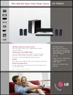
Summary of Contents for DMR-ES35VP

Page 1: ... Matsushita Electric Industrial Co Ltd All rights reserved Unauthorized copying and distribution is a violation of law DMR ES35VP DMR ES35VPC Vol 1 Colour S Silver Type DVD Recorder ORDER NO VR0603001CE B24 ...

Page 2: ...65 13 4 Analog Timer Block Diagram 66 13 5 System Control Servo Block Diagram 67 14 Schematic Diagram 69 14 1 Interconnection Schematic Diagram 69 14 2 Power Supply Section Power Digital I F P C B 1 2 Schematic Diagram P 71 14 3 Digital I F 1 4 Section Power Digital I F P C B 2 2 Schematic Diagram IF 73 14 4 Digital I F 2 4 Section Power Digital I F P C B 2 2 Schematic Diagram IF 74 14 5 Digital I...

Page 3: ...ack P C B FL Drive P C B 103 16 Exploded Views 105 16 1 Casing Parts Mechanism Section1 105 16 2 Casing Parts Mechanism Section 2 106 16 3 VHS Mechanism Section 107 16 4 Packing Accessories Section 108 17 Replacement Parts List 109 3 DMR ES35VP DMR ES35VPC ...

Page 4: ...sure the potential across the resistor 4 Check each exposed metallic part and measure the voltage at each point 5 Reverse the AC plug in the AC outlet and repeat each of the above measurements 6 The potential at any point should not exceed 0 75 volts RMS A leakage current tester Simpson Model 229 or equivalent may be used to make the hot checks leakage current must not exceed 1 2 milliampere In ca...

Page 5: ...y 3 Use only a grounded tip soldering iron to solder or unsolder ES devices 4 Use only an anti static solder removal device Some solder removal devices not classified as anti static ESD protected can generate electrical charge sufficient to damage ES devices 5 Do not use freon propelled chemicals These can generate electrical charges sufficient to damage ES devices 6 Do not remove a replacement ES...

Page 6: ...2 2 Precaution of Laser Diode 6 DMR ES35VP DMR ES35VPC ...

Page 7: ...Solder PbF The lead free solder has to be used when repairing the equipment for which the lead free solder is used Definition The letter of PbF is printed on the PCB using the lead free solder To put lead free solder it should be well molten and mixed with the original lead free solder Remove the remaining lead free solder on the PCB cleanly for soldering of the new IC Since the melting point of t...

Page 8: ...3 Service Navigation 3 1 Service Information 8 DMR ES35VP DMR ES35VPC ...

Page 9: ...4 Specifications 9 DMR ES35VP DMR ES35VPC ...

Page 10: ...5 Location of Controls and Components 5 1 Each Buttons 10 DMR ES35VP DMR ES35VPC ...

Page 11: ...11 DMR ES35VP DMR ES35VPC ...

Page 12: ... DVD When the power can not be turned off 1 Press POWER key on the front panel for over 10 seconds to turn off the power forcibly and press STOP CH UP keys on the front panel simultaneously for 5 seconds 6 1 2 DVD When the Forcible Disc Eject can not be done 1 Turn off the power and pull out AC cord 2 Remove the Top Case 3 Push in SLIDE CAM by Eject Pin JSJ0484 or minus screw driver small to eject...

Page 13: ...es 1 Disconnect the AC plug and remove the Top Panel and the Front Panel by referring to the Disassembly Procedures 2 Connect three batteries 1 5V spec to the Loading Motor in series for supplying 4 5V to rotate the Loading Motor as shown below 3 Stop unloading just before unloading will be completed as shown below and then the tape becomes slack as shown below 4 Rotate the S Reel by a small minus...

Page 14: ...tan Motor clockwise to remove the slack tape as shown below 5 Rotate the Main Cam Gear counter clockwise again to remove the cassette tape as shown below 6 Attach Loading Motor and tighten the screw 7 Set the Position Switch to EJECT POSITION certainly and attach the mechanism to chassis as shown below 14 DMR ES35VP DMR ES35VPC ...

Page 15: ...ecovery process No display U88 The unit is carrying out its recovery process No display U99 Hang up Displayed when communication error has occurred between Main microprocessor and Timer microprocessor No display Displayed is left until the POWER key is pressed H19 Inoperative fan motor When inoperative fan motor is detected after powered on the power is turned off automatically The event is saved ...

Page 16: ...tted DVD RAM or DVD RW that is unformatted or recorded on other equipment 7 1 2 DVD Special Modes Setting Item FL display Key operation Mode name Description Front Key TEST Mode All the main unit s parameters include tuner are initialized Press VHS to DVD DUBBING REC and OPEN CLOSE keys simultaneously for five seconds when power is off Rating password The audiovisual level setting password is init...

Page 17: ...g Contents Example Demonstration lock unlock Ejection of the disc is prohibited The lock setting is effective until unlocking the tray and not released by Main unit initialization of service mode When lock the tray LOCK is displayed for 3 seconds When the power is on press STOP and POWER keys simultaneously for 5 seconds Note When a disc is not in tray this setting is not effective When unlock the...

Page 18: ...ess 0 2 in service mode White Picture Output White picture is output as component Output from AV Decoder White picture Saturation rate 100 It is enable to switch Interlace Progressive by I P switch 1 4 Initial mode is Interlace Press 1 1 in service mode Switch Interlace Progressive Press 1 4 in White Picture Output mode I P are switched alternately Magenta Picture Output Magenta picture is output ...

Page 19: ...s applied normally by the Digital P C B Press 2 2 in service mode Audio Pattern Output The audio pattern stored in the internal memory is output Lch 1kHz 18dB Rch 400Hz 18dB Audio sound clock switching operation of DAC can be confirmed by sub command 2 4 Initial mode Audio 48kHz Press 2 3 in service mode Audio 44 1kHz 48kHz switching Press 2 4 in Audio Pattern Output mode 48 kHz 44 1 kHz are switc...

Page 20: ... be identified display is black out Delete the Last Drive Error Delete the Last Drive Error information stored on the DVD RAM Drive Press 9 6 in service mode Laser power confirmation Drive state is judged based on difference between laser power value at shipping and present laser power value If DVD RAM disc in not inserted NO DISC is displayed If power value study was filed ERROR is displayed 1 in...

Page 21: ...4 Defect of Digital P C B or Communication Error 05 Defect of Digital P C B AV DEC MAIN CPU Display the time when the error has occurred for 5 seconds DD Day hh Hour mm Minute Accumulated working time till occuring of the error is left displayed Indicating unit Second Press 6 5 in service mode Then press 0 1 1 9 the past 19 error histories are displayed Delete the Error History Delete Error Histor...

Page 22: ...peration Mode name Description Remote controller key Finishing service mode Release Service Mode Display in STOP E E mode Press power button on the front panel or Remote controller in service mode 22 DMR ES35VP DMR ES35VPC ...

Page 23: ...der could not be started Error of the cylinder or the cylinder driver Yes Yes H02 The CAP FG could not be detected Yes Yes F03 Mechanism lock during without the unloading and the cassette up Yes Yes F04 Mechanism lock during unloading Yes Yes F05 S reel pulse cannot be detected when a cassette tape is inserted Error of the S reel system or the Capstan system No Yes F06 Mechanism lock during the Ca...

Page 24: ... SELECT to VHS When power is OFF press STOP and EJECT keys simultaneously for 3 seconds to into Service Mode In Service Mode press STOP and EJECT keys simultaneously to add Service Number 7 2 3 1 VHS Service Mode and Service Data at a glance Service Number Contents Contents of Indication on minute Contents of Indication on second Remarks 0 Indication for the inner data of IC6001 VHS mode Real time...

Page 25: ...plementary data 1 and 2 of history 2 In these modes the supplementary data 3 and 4 instead of the Error number and supplementary data 1 and 2 are indicated only while pressing STOP key 5 Self diagnosis history 3rd Error number of history 3 Supplementary data 1 and 2 of history 3 6 Indication for the inner data of IC6001 Real time servo data 4 digits Real time Higher rank 1 BYTE of SERVO data Lower...

Page 26: ...ple of Display A Service Mode Number B Supplementary Data 3 Mechanism process shifting Number C Supplementary Data 4 LM Loading Motor information Display of means that Loading Motor turns ON when EJECT button was pressed but an error has occurred while mechanism was between REV position and LOAD position Supplementary Data 3 EJECT FF REW 10 PLAY passing REV 11 passing REV 12 passing REV LOAD Capst...

Page 27: ...ot be detected when a cassette tape is inserted Error of the S reel system or the Capstan system VHS mode Value of S Reel Pulse counted Process No 16 Detection of the Cylinder lock during the constant rotation VHS mode Tape position Process No 17 Detection of S reel lock during the constant tape running VHS mode Tape position Process No Number of FG 18 Detection of T reel lock during the constant ...

Page 28: ...exadecimal A 10 Decimal E 14 Decimal Hexadecimal indication from A to E are shown below Note 3 Supplementary Data 2 Reason of Ejection Supplementary Data 2 Reason 1 S reel pulse is less than 3 when the loading has been completed Miss catching the tape 2 Pulse Timer over during the short rewind at the DOWN position Error of S photo sensor system S reel system Capstan system 3 Mechanism lock from th...

Page 29: ...ck P C B 10 Pin Same as E75V ES30V Series RFKZ0365 Extension Cable Main P C B RAM Digital P C B Module 64 Pin Same as ES15 Series JZS0484 Eject Pin Same as ES15 E50 Series RFKZ03D01K Lead Free Solder 0 3mm 100g Reel Same as ES15 Series RFKZ06D01K Lead Free Solder 0 6mm 100g Reel Same as ES15 Series RFKZ10D01 Lead Free Solder 1 0mm 100g Reel Same as ES15 Series RFKZ0316 Solder Remover Lead free 10W...

Page 30: ...mbly Flow Chart The following chart is the procedure for disassembling the casing and inside parts for internal inspection when carrying out the servicing To assemble the unit reverse the steps shown in the chart below 30 DMR ES35VP DMR ES35VPC ...

Page 31: ...9 2 P C B Positions 31 DMR ES35VP DMR ES35VPC ...

Page 32: ...e1 For description of the disassembling procedure see the section 9 4 Note2 Video Cassette might not enter when a strong lighting is applied to VHS Mechanism when Video Cassette is inserted Please weaken the lighting or cover with the top panel etc 32 DMR ES35VP DMR ES35VPC ...

Page 33: ...ar side of the Top Case a little and lift the Top Case in the direction of the arrows 9 5 Front Panel 1 Remove one screw A 2 Unlock tab A and tab B simultaneously 3 Unlock tab C and tab D simultaneously 4 Unlock 2 tabs E respectively and pull out Front Panel with connector slightly 33 DMR ES35VP DMR ES35VPC ...

Page 34: ...P C B FL Drive P C B 1 Remove 5 screws A to remove FL Drive P C B 2 Remove 3 screws B and unlock Locking Tab A to remove Front Jack P C B 9 7 RAM Digital P C B Module 1 Remove 3 Screws A 2 With holding DVD drive as below illustration remove 3 Screws B and disconnect FFC And lift up Digital P C B slightly so to disconnect connectors to remove Digital P C B 34 DMR ES35VP DMR ES35VPC ...

Page 35: ...n RAM Drive and remove RAM Digital P C B Module Note RAM Digital P C B Module as service part has no heat sink unit Before returning to customer heat sink unit should be installed on Digital P C B 35 DMR ES35VP DMR ES35VPC ...

Page 36: ...B Screw C and Screw D 3 Lift up VTR Mechanism Unit perpendicularly so to disconnect Connectors P2571 and P3001 Note Pay attention to stiff connections of P2571 and P3001 when removing VTR Mechanism Unit 9 9 1 Caution for attaching VTR Mechanism Unit 1 Attach VTR Mechanism Unit so that Boss of Position SW is put into long hole of Main Cam Gear refer to Fig B 36 DMR ES35VP DMR ES35VPC ...

Page 37: ... Fan Motor 1 Disconnect Fan Connector 2 Remove 6 Screws A and 1 Screw B 3 Unlock 2 Locking Tabs A to remove Rear Panel with Fan Motor 9 10 1 1 Only Fan Motor 1 Disconnect Fan Connector 2 Remove 2 Screws A to Remove Fan Motor 37 DMR ES35VP DMR ES35VPC ...

Page 38: ...9 11 Power Digital I F P C B 1 Disconnect 5 Connectors A 2 Remove the 2 Screws A 3 Remove Power Digital I F P C B 38 DMR ES35VP DMR ES35VPC ...

Page 39: ...9 12 Main P C B 1 Disconnect 5 Connectors 2 Remove 2 Screws A and remove Main P C B 39 DMR ES35VP DMR ES35VPC ...

Page 40: ...Measurements and Adjustments 10 1 Service Positions Note For description of the disassembling procedure see the section 9 10 1 1 Checking and Repairing of Power Digital I F P C B 40 DMR ES35VP DMR ES35VPC ...

Page 41: ...10 1 2 Checking and Repairing of Main P C B 41 DMR ES35VP DMR ES35VPC ...

Page 42: ...10 1 3 Checking and Repairing of RAM Digital P C B Module 42 DMR ES35VP DMR ES35VPC ...

Page 43: ...0 2 Caution for Replacing Parts 10 2 1 Notice for replacing parts of VHS Mechanism 10 2 1 1 Regarding change of parts of VHS mechanism 10 2 2 Notice for Replacing Capstan Motor 43 DMR ES35VP DMR ES35VPC ...

Page 44: ...10 2 3 Items that should be done after replacing parts 44 DMR ES35VP DMR ES35VPC ...

Page 45: ...45 DMR ES35VP DMR ES35VPC ...

Page 46: ...e is caused by DV terminal Models with DV Input Jack 1 DV terminal Check to be able to record from DVC 7 After checking and making repairs upgrade the firmware to the latest version Make sure that FIRM_SUCCESS appears in the FL displays UNSUPPORT display means the unit is already updated to newest same version Then version up is not necessary 8 Transfer 9 9 in the service mode setting and initiali...

Page 47: ... BIAS DROP OUT SIGNAL DATA REQUEST DATA RESPONSE DIGITAL SERVO CONTROLLER DATA SLICE LOOP FILTER DIGITAL VIDEO DISC INITIAL LOGO ABBREVIATIONS E EC ECR ENCSEL ETMCLK ETSCLK ERROR TORQUE CONTROL ERROR TORQUE CONTROL REFERENCE ENCODER SELECT EXTERNAL M CLOCK 81MHz 40 5MHz EXTERNAL S CLOCK 54MHz F FBAL FCLK FE FFI FEO FG FSC FSCK FOCUS BALANCE FRAME CLOCK FOCUS ERROR FOCUS ERROR AMP INVERTED INPUT FO...

Page 48: ...L SUB CODE CLOCK SUB CODE Q DATA SYSTEM CLOCK T TE TIBAL TID TIN TIP TIS TPSN TPSO TPSP TRCRS TRON TRSON TRACKING ERROR BALANCE CONTROL BALANCE OUTPUT 1 BALANCE INPUT BALANCE INPUT BALANCE OUTPUT 2 OP AMP INPUT OP AMP OUTPUT OP AMP INVERTED INPUT TRACK CROSS SIGNAL TRACKING ON TRAVERSE SERVO ON INITIAL LOGO ABBREVIATIONS V VBLANK VCC VCDCONT VDD VFB VREF VSS V BLANKING COLLECTOR POWER SUPPLY VOLTA...

Page 49: ...UDIO OUTPUT L AUDIO OUTPUT R AUDIO SELECT H AUDIO L AUDIO R AV CONTROL AV CONTROL AV CONTROL SERIAL CLOCK AV CONTROL MODE AV CONTROL LEVEL METER R AV SW LEVEL METER L B MODE H BURST GATE PULSE BACK UP 5V BAND U BAND VL BILINGUAL MIX L BIL BIL L BIL H BIL M1 L BS CLOCK BS DATA BS LCH IN BS MIX H BS MON H BS MONI H BS RCH IN BS VIDEO BS VIDEO BS1 BS H BS LEVEL BS M H BS VTR H BUS CLK BUS LSN BUS TLK...

Page 50: ...TE H FM OUTPUT L FM OUTPUT R FM PACK OUTPUT L FM PACK OUTPUT R FM BS SELECT L FM BS SELECT R FS CLOCK FULL ERASE HEAD ON H FULL ERASE HEAD ON H FULL E 12V GND A GND TU GND N SW 12V H SYNC H AMP SW H P R H P L H P GND H P OUT L H P OUT R H SW HEAD PHONE L HEAD PHONE R HEAD SW HEATER HEATER HSS HTR HTR I RFE ICL IF IN SELA1 IN SELA2 IN SELA3 INS L R L INS H INSEL A1 INSEL A2 INSERT INSERT H IO CS JO...

Page 51: ...MAL H NR BIAS NTSC L CONTROL AGC CIRCUIT OUTPUT P OFF H P OFF L P FAIL P OFF H P OFF L PAL H PAL L NTSC H PB ADJ OUT PB OUT PB H PFG PHOTSN B PICT CNT PLAY LED RVS LED PLAY PO PLAY R LED PLY DEW POWER OFF L PREROLL H PWRFAIL R CH H R CH L R ST R S F RCH H REC 12V REC CHROMA REC H REC IN REC OUT L REC START REC VR C REC VR L REC VR R REC Y REC H REC C REC Y REC EE CTL REEL T REEL S REGULATOR FILTER...

Page 52: ... STOP 2 POSITION STOP 2 POSITION SAFETY TAB SW STEREO H SUB BIAS SUB SW S VHS CASSETTE L SW 5V DETECT SYNC L SYSCON 5V SYSTEM T PHOTO T RL PLS T BUSCLK T BUSLSN T BUSTLK T END L T PHOTO TAPE END L TAPE END L CAM TEST TPZ TRIC L TRICK L TRK ENV TU AUDIO TU GND TU V IN TU VIDEO TUN NOR IN TUN R TUN AUDIO IN TUNER 12V TUNER L TUNER V IN TUNER L TUNER N TUNER R TUNER 12 TUOFF H TV AUDIO TV VTR TXTON L...

Page 53: ... 2 5 5 7 0 1 2 7 0 1 2 7 4 0 7 7 7 6 7 7 7 6 6 6 6 3 3 6 0 3 89 0 7 7 7 6 7 7 7 6 6 6 6 3 3 6 0 3 8 0 7 7 7 6 7 7 7 6 6 6 6 3 3 6 0 3 0 4 6 2 0 3 0 6 89 6 2 0 3 0 6 8 6 2 0 3 0 6 4 4 7 7 2 7 6 0 0 6 6 2 7 6 89 7 7 2 7 6 0 0 6 6 2 7 6 8 7 7 2 7 6 0 0 6 6 2 7 6 0 1 2 7 0 1 4 1 1 1 1 1 1 1 1 3 3 0 2 1 6 6 89 1 1 1 1 1 1 1 1 3 3 0 2 1 6 6 8 1 1 1 1 1 1 1 1 3 3 0 2 1 6 6 0 1 4 4 4 0 0 2 2 0 0 2 3 3 89 ...

Page 54: ...1 0 2 6 89 0 2 1 0 2 6 8 0 2 1 0 2 6 0 1 2 7 3 6 0 1 2 7 3 6 4 6 6 7 6 6 7 7 6 2 0 6 2 3 6 6 89 6 6 7 6 6 7 7 6 2 0 6 2 3 6 6 8 6 6 7 6 6 7 7 6 2 0 6 2 3 6 6 0 1 2 7 3 6 0 1 2 7 3 6 4 0 0 6 6 6 0 0 6 0 6 6 0 6 0 6 89 0 0 6 6 6 0 0 6 0 6 6 0 6 0 6 8 0 0 6 6 6 0 0 6 0 6 6 0 6 0 6 0 1 2 7 3 06 0 0 0 0 00 01 02 07 03 16 4 6 3 3 0 3 0 6 6 0 0 3 6 0 6 0 1 1 1 89 6 3 3 0 3 0 6 6 0 0 3 6 0 6 0 1 1 1 8 6 3...

Page 55: ...9 0 6 5 2 0 6 2 5 8 0 6 5 2 0 6 2 5 0 1 2 7 4 0 6 5 6 3 5 5 0 2 89 0 6 5 6 3 5 5 0 2 8 0 6 5 6 3 5 5 0 2 0 1 2 7 3 6 0 1 2 7 3 6 4 7 7 6 7 7 7 2 7 7 5 5 6 6 7 7 7 6 6 89 7 7 6 7 7 7 2 7 7 5 5 6 6 7 7 7 6 6 8 7 7 6 7 7 7 2 7 7 5 5 6 6 7 7 7 6 6 0 1 2 7 3 6 0 1 2 7 3 6 4 6 1 2 3 7 7 7 6 0 7 2 7 7 7 7 6 6 7 5 1 7 89 6 1 2 3 7 7 7 6 0 7 2 7 7 7 7 6 6 7 5 1 7 8 6 1 2 3 7 7 7 6 0 7 2 7 7 7 7 6 6 7 5 1 7...

Page 56: ... 6 6 1 6 6 7 6 1 89 0 0 6 6 6 0 2 6 6 6 1 6 6 7 6 1 8 0 0 6 6 6 0 2 6 6 6 1 6 6 7 6 1 0 0 4 4 6 6 56 6 56 0 0 7 0 7 6 6 6 0 7 56 0 0 7 89 6 6 56 6 56 0 0 7 0 7 6 6 6 0 7 56 0 0 7 8 6 6 56 6 56 0 0 7 0 7 6 6 6 0 7 56 0 0 7 0 0 4 4 6 6 56 6 56 0 6 6 56 6 56 1 7 2 6 89 6 6 56 6 56 0 6 6 56 6 56 1 7 2 6 8 6 6 56 6 56 0 6 6 56 6 56 1 7 2 6 0 4 4 4 4 6 6 2 6 2 6 56 1 6 1 6 0 1 1 6 89 6 6 2 6 2 6 56 1 6 ...

Page 57: ... 2 0 8 1 7 1 6 7 6 0 0 0 6 7 0 2 0 0 1 2 7 3 6 0 1 2 7 3 6 4 6 6 6 0 5 0 6 1 6 6 6 3 6 6 0 7 89 6 6 6 0 5 0 6 1 6 6 6 3 6 6 0 7 8 6 6 6 0 5 0 6 1 6 6 6 3 6 6 0 7 0 1 2 7 3 06 0 0 0 0 00 01 02 07 03 16 4 6 6 6 3 6 6 3 3 6 3 6 0 6 6 3 6 3 89 6 6 6 3 6 6 3 3 6 3 6 0 6 6 3 6 3 8 6 6 6 3 6 6 3 3 6 3 6 0 6 6 3 6 3 1 1 1 1 4 6 0 6 89 6 0 6 8 6 0 6 80366 80366 80366 80366 57 DMR ES35VP DMR ES35VPC ...

Page 58: ...LAY 0 2Vp p 20usec div IC3001 80 REC PLAY 0 5Vp p 10msec div IC4501 21 TW4501 REC 1 1Vp p 20usec div IC3001 86 REC 1 4Vp p 20usec div IC6001 80 FF REW 5 0Vp p 1msec div IC6001 95 REC 2 4Vp p 10msec div IC3001 6 REC PLAY 0 9Vp p 2msec div IC3001 19 REC 1 0Vp p 20usec div IC3001 29 REC PLAY 2 4Vp p 20usec div IC3001 36 PLAY 0 5Vp p 20usec div IC4501 57 REC PLAY 1 6Vp p 0 5msec div IC4501 53 REC PLAY...

Page 59: ...25Vp p 5usec div T11301 6 STOP 300Vp p 5usec div T11101 4 STOP 36Vp p 5usec div P59001 43 REC PLAY 0 8Vp p 20usec div P59001 59 REC PLAY 1 0Vp p 20usec div P59001 51 REC PLAY 1 0Vp p 20usec div P59001 55 REC PLAY 0 6Vp p 20usec div P59001 39 REC PLAY 1 0Vp p 20usec div P59001 17 19 REC PLAY 0 8Vp p 1msec div JK3902 3 REC PLAY 2 0Vp p 20usec div JK3902 4 REC PLAY 1 5Vp p 20usec div JK3902 16 REC PL...

Page 60: ...60 DMR ES35VP DMR ES35VPC ...

Page 61: ... 1 2 IP11703 1 2 A IC11502 ERROR VOLTAGE DET 1 K R 3 ERROR VOLTAGE DET VCC 4 D11305 GND 3 D11304 D11306 IC11301 F B DRAIN 5 2 ZC SWITCHING IC 1 3 R K 1 1 2 4 IC11701 3 FEED BACK Q11301 A 2 D11212 D11203 D11210 B1 20 19 18 17 16 15 14 13 12 9 8 B2 6 P2 4 P1 B2 B1 P2 P1 11 9 5 4 3 1 1 P6001 P31905 DMR ES35VP PC Power Supply Block Diagram 1 2 4 3 FEED BACK Q11101 VCC 7 4 1 2 3 GND 3 HOT COLD IC11201 ...

Page 62: ...2001 V IN REG A 5V A 5V 5V ON 3 V OUT 5 4 IC45001 V IN REG AU 5V D S G 4 5 DR 12V SELECT SWITCH Q11601 8 3 7 2 1 6 DC DC CONVERTER IC11801 DC DC CONVERTER IC11601 5 7 2 1 FB ON OFF V IN EXT D REG D 12V D Q11801 G S D D 3 6 2 5 4 1 DI P ON OUT QR11602 QR11603 5 7 2 1 FB EXT ON OFF V IN Q11602 REG DR 5V TO IC3701 FROM IC7501 D D G D D S 1 2 3 6 5 4 ON OFF 1 V OUT 9V JC POWER ON 4 55 5 IC4801 REG 9V ...

Page 63: ... LPF 6 7M VIDEO OUT COMPONENT P37101 P37101 P37101 P37101 P37101 JK3802 DVD L1 L2 SW DET 6 S VIDEO IN L2 1 2 6 5 3 4 S VIDEO IN 6 5 REAR A V OUT JACK JK4801 OUT COMMON VHS DVD DVD PR RED 18 PB BLUE 19 Y GREEN 20 IC37501 IIC CLOCK IC37501 IIC DATA SYSTEM CONTROL SECTION TO FROM V1 OUT Pr R C OUT Py G OUT Y75 OUT Y C MIX C75 SAG DVD R Pr IN DVD B Pb IN DVD G Py IN DVD Y IN DVD C IN CONTROL IIC BUS S...

Page 64: ... SQPB SQPB P R Y LPF R P GCL TO C CCD P EQ SQPB DL SQPB DET S PB DRIVER C CLOCK 2FSC OSCILLATOR VCO X TAL PB AGC APL REC FBC ALC ADJUSTMENT fo DEVIATION ET LPF MODULATION FM P FILTER REC DE EMPHASIS MAIN ACC DET CHROMA R ACC DET W C D C CARRIER OFFSET MAIN EMPHASIS ACC SW TRAP 629MHz REC APC LPF SUB KILLER SQPB PB APC DEMO APC SW AGC FM EQ SQPB DLIM DE EMPHASIS NON LINEAR VIDEO ALC G EQ CLAMP FEED...

Page 65: ... P3001 P3001 7 P3001 FM MIX TW4501 ENVE TW4502 IC3001 AUDIO PROCESSOR 3 P4002 4 P4002 AMP PRE EQ REC TRAP fh VCA P R 96 98 6 2 43 42 DVD R DVD L 64 15 10 14 63 9 22 24 29 27 21 30 57 53 62 61 VHS L VHS R ADC L LINE OUT R LINE OUT L ADC R DVD OUT L DVD OUT R P C B DIGITAL TO P59001 P59001 19 P37101 17 P37101 24 20 L OUT R OUT REAR OUTPUT JACK JK3902 DVD P6004 P31902 P6004 5 2 P31902 27 P37101 P5900...

Page 66: ...P31905 PS31901 PP7701 P6001 P31905 PS31901 PP7701 P6001 P31905 PS31901 PP7701 P6001 P31905 PS31901 PP7701 P6001 P31905 13 12 11 TIMER DISPLAY VDD FAN LOCK 88 OUT FAN PWM 94 MAIN P C B FRONT R P C B TIMER CPU DP7501 34 4 41 1GA 38 1GA 35 1GA 11 1GB 8 1GB 5 1GB 33 2G 31 2G 29 3G 27 3G 26 4G 23 4G 22 5G 20 5G 18 6G 16 6G 14 7G 12 7G P16 P1 32 P2 30 P3 28 P4 25 P5 24 P6 21 P7 19 P8 17 P9 15 P10 13 P11...

Page 67: ...7 SAFETY TAB 7 S PHOTO 8 T PHOTO SW MODE S1532 5 4 3 2 1 SW4 SW3 SW2 SW1 SW4 SW3 SW2 SW1 30 POSITION SW4 POSITION SW3 31 32 POSITION SW2 POSITION SW1 33 PB CTL OUT EX FF REW TW2002 97 82 6 5 P4002 1 P1531 2 P1531 P4002 HEAD CONTROL 95 94 COMPOSER FG PG AMPLIFIRE DIFFERENTIAL 17 16 15 CYL PFG 90 18 CYL ET CTL AMP REF 96 O REF 91 UNLOADING LOADING CAP FG IN CAP FG OUT 77 14 AMPLIFIRE DIFFERENTIAL CO...

Page 68: ...DMR ES35VP DMR ES35VPC 68 ...

Page 69: ...CER VIDEO IECOUT AU GND MIX R OUT DM P SAVE MIX L OUT DM XDMUTE L COUT DM V YIN DM AU GND GND GND GND UNREG 38V CPNCIN DM X SW12 3V SLICER VIDEO AU GND MIX R OUT DM P SAVE 3 4 2 5 1 6 7 6 8 9 11 10 8 9 11 10 13 12 15 14 15 14 11 10 9 8 7 6 1 5 2 4 3 PP7701 10 9 8 7 6 5 4 3 2 1 1 6 5 4 3 2 GND GND KEY1 KEY2 KEY3 SST6V I2C5 DT I2C5 DT I2C5 CK I2C5 CK PS31901 1 6 5 4 3 2 GND GND KEY1 KEY2 KEY3 SST6V ...

Page 70: ...USY DGND ANA3 3V CSYNC IN P OFF L3 UARTP2M UARTM2P DGND DGND DGND IECOUT MIXROUT DM MIXLOUT DM IT CK 64 63 62 61 60 59 58 57 56 55 54 53 52 51 12 50 10 14 13 11 1 15 9 8 16 7 6 17 5 4 18 3 2 19 20 21 22 23 24 25 26 27 28 29 30 31 32 33 34 35 36 37 38 39 40 41 42 43 44 45 46 47 48 49 AADC R XFWE D1 2V COUT DM DGND YOUT DM DGND DGND X SW 3 2V D3 3V I2C5CK AU5V ITM2A SCLK XINTP DR12V DR12V XINTM DRGN...

Page 71: ...L11801 1 2 5 6 3 4 Q11801 B1DHDD000022 VWJ0795 5 L11705 G0A100HA0023 L11704 D_P_OFF_L1 D12V 22K 22 R11704 C11712 ECJ2VB1E473K A R 3 2 C 1 C0DAEJC00006 C0DAEMB00003 IC11701 C11711 0 1 KB 22 F2A1C5610006 C11703 2400 G 22 R11706 820 G 22 R11707 F2A1H5600018 C11704 L11703 G0A100HA0023 F2A1C1210017 C11707 J0JHC0000048 LB11703 D11703 B0AADM000003 C11205 ECJGVB1H102K C11204 0 1 KB 22 13K G 22 R11203 MAZ7...

Page 72: ...ARTUP OFF CIRCUIT START UP CC VREF SS V5 PWON VIN FB GND EXT CS COMP CNT SHIFT LEVEL UVLOcomp VREF 0 8V V5 RESET CONTROL LOGIC 8 7 6 5 4 3 2 1 NC NC NC CONT VIN VOUT GND CN SHUTDOWN THERMAL LIMITTER CURRENT DRIVER BIAS REFERENCE 8 7 6 5 4 3 2 1 CC VREF SS PWON VIN FB GND EXT CS COMP CNT SHIFT LEVEL UVLOcomp VREF 0 8V V5 RESET CONTROL LOGIC 8 7 6 5 4 3 2 1 IC11301 SWITCHING IC IC DETAIL BLOCK DIAGR...

Page 73: ...UT1 or B IN V B OUT B IN NR VOUT P GND P DGND IECOUT GND GND I2C5_CK GPYOUT_DM Y_OUT_DM BPBOUT_DM RPROUT_DM TO P6005 MAIN P C B SYSCON SERVO TIMER SECTION TO P6004 MAIN P C B SYSCON SERVO TIMER SECTION TO P6003 MAIN P C B SYSCON SERVO TIMER SECTION I2C5_DT BS16V DR_PSAVE_L UARTM2P IR_TXD BBR_RXD IR CLK BS_P_ON_H ADC_R GND GND GND ADC_L X_SW6V X_SW6V MGND AU_GND AU_GND P_SAVE ANA5V D3R3V FANPWM1 DI...

Page 74: ...SCON SERVO TIMER SECTION TO PP7701 FRONT R P C B HDMI_MONI HOT_PLUG GND F GND IR GND F 29V GND KEY3 KEY1 KEY2 AD5V SST6V SD_LED DUB_LED DVD_LED VHS_LED GND HDMI_P3_ON_H HDMI_P5_ON_H HDMI_CONT POFF_L2 SCLK POFF_L3 UARTP2M RST_UART IR_CS SW_UART IR_BUSY SBMTP BODY 12 XMPREQ HDD_PFAIL SBPTM XFWE XINTP XINTM 1 3 4 5 6 7 8 9 10 11 12 AE AF AG AH AI AJ AK AL AM AN AO AP AQ AR AS NOTE DO NOT USE THE PART...

Page 75: ...25 B 5 4 3 2 1 C B A B TO DIGITAL I F SECTION 1 4 NOTE DO NOT USE THE PART NUMBER SHOWN ON THIS DRAWING FOR ORDERRING THE CORRECT PART NUMBER IS SHOWN IN THE PARTS LIST AND MAY BE SLIGHTLYDIFFERNT OR AMENDED SINCE THIS DRAWING WAS PREPARED LOCATION MAP 1 4 2 4 3 4 4 4 DMR ES35VP PC Digital I F 3 4 Section Power Digital I F P C B 2 2 Schematic Diagram IF P Power Supply Section Page A IF Digital I F...

Page 76: ...1001 C37013 0 1 KB C31506 F1H0J1050010 C31507 F1H0J1050010 C31508 0 01 KB 6 7 5 2 4 3 8 1 IC31503 C3EBFC000053 ERJ3GEY0R00V LB37006 LB37013 J0JKB0000032 LB37005 J0JKB0000032 P P P TO P59001 DIGITAL P C B MODE SELECT SECTION CSYNC_IN D3R8V D3R8V ANA3R3V EPG_ON_H BUSY DR5V XFWE DR5V DGND DGND DGND DGND DGND DGND D3R3V ITA2M I2C5DT IT_CK I2C5CK DR12V DR12V DRGND ITM2A DRGND DGND IECOUT P_OFF_L2 X_SW_...

Page 77: ...3 0 Q4082 2SD0602ARL C4084 1800P C4081 22n C4083 6V47 4 3 2 1 6 G2A472C00003 T4081 S S S S S S S V OUT S I S S S S S V IN ON H NC GND 9 8 7 6 5 4 3 1 2 NOTE DO NOT USE THE PART NUMBER SHOWN ON THIS DRAWING FOR ORDERRING THE CORRECT PART NUMBER IS SHOWN IN THE PARTS LIST AND MAY BE SLIGHTLYDIFFERNT OR AMENDED SINCE THIS DRAWING WAS PREPARED 5 4 3 2 1 C B A C TO VIDEO SECTION 3 4 LOCATION MAP 1 4 2 ...

Page 78: ...T_NORMAL IN_NORMAL 1500 R3001 FULL E A E IN GND E A HEAD R A HEAD W CTL HEAD A A A CTL HEAD FULL E VIDEO ENVE FM_MUT MESECAM Det MIX LEVEL SW37 ADJUST REC SW44 DET DET Mute SP2 LPF B E L SECAM SW39 CCD CONT Color Level EVVDET HPF P R SW50 DETERTOR TANK CR DET COMO B Y Invert ACC VCA SW40 INT SP SW48 SW49 SW47 CH1 SP2 SP2 SP2 SW41 CH2 SW43 SP2 SP EXT INT SW38 R HPF 2MLPF L SECAM SP2 CH1 SP2 SW45 CH...

Page 79: ... 2 3 4 5 6 7 8 9 10 11 12 13 14 15 16 17 18 19 20 21 22 5 4 3 2 1 C B A C TO VIDEO SECTION 1 4 NOTE DO NOT USE THE PART NUMBER SHOWN ON THIS DRAWING FOR ORDERRING THE CORRECT PART NUMBER IS SHOWN IN THE PARTS LIST AND MAY BE SLIGHTLYDIFFERNT OR AMENDED SINCE THIS DRAWING WAS PREPARED LOCATION MAP 1 4 2 4 3 4 4 4 DMR ES35VP PC Video 3 4 Section Main P C B 1 4 Schematic Diagram V V Video Section Pag...

Page 80: ...R SW34 fh HPF CTL Trap SD 6dBAMP De Emph SSEQ SW17 Delay Y LPF SQPB EQ N L C Sque lch P SVHS L SECAM SW15 P C K L Det R LPF C CCD R SW30 SW29 R P CCD CLPF2 SW33 CLPF1 4Phase 2fsc Y CCD Down LCVCO Clock Driver Conv ACC Dst REC AFC Discri Control Mode VCA P ACC Det ACC SW CCD CONT Chroma SW51 B D C K NP Conv SW26 Pilot R L SECAM Pilot Add INT EXT BPF P P R P SW27 Erase Main Conv2 Conv1 Main R P R el...

Page 81: ..._L 23 58 45 44 47 48 46 30 31 32 43 40 41 35 37 36 33 34 39 38 42 28 25 26 24 27 29 55 56 50 51 49 53 54 52 57 62 63 61 19 18 20 3 2 5 4 6 8 7 1 64 15 16 9 13 10 12 11 14 17 22 21 59 60 AN3656NFBPBV IC4501 V V S S S V S S V V V V I I S S I EXT4 EXT4 FM MIX ENVE I S TV TV L SW22 MIX MUTE SW19 R SW21 AGC SW20 SW18 MIX HIFI PNR Rch R HIFI L L R MUTE NORMAL L SW16 MIX NORMAL SW17 VCC 5V LOGIC GND DATA...

Page 82: ... 32 31 36 38 25 40 42 44 13 46 MN67788RD IC7501 2SD132800L Q7501 47K R7530 R7527 VWJ0795 5 ERJ3GEYJ103V R7537 47K R7532 47K R7540 47K R7533 47K R7528 47K R7531 DR_SAVE S2 S1 G5 S6 S5 G4 S3 S4 S9 G6 S7 S8 S11 G7 S10 23 21 16 17 14 15 19 20 18 13 22 44 39 35 31 26 27 24 25 30 28 29 34 32 33 38 36 37 42 40 41 45 DP7501 A2BD00000155 SD_SEL PSAVEH HOT_PLUG S12 S9 S7 S6 S8 S11 S10 NC S15 S16 BS_H L3_H S...

Page 83: ... TL23 D1501 B3EA00000072 DGND I2C5_CK GND GND GND YOUT_DM BPBOUT_DM IECOUT GPYOUT_DM RPROUT_DM I2C5_DT V I I I I I I I I I I A V I I I I I I I I V V SCLK IR_CLK BS_P_ON_H S PHOTO BS16V SENSOR UARTM2P IR_TXD BBR_RXD S REEL MGND MECHA_12R3V ADC_L ADC_R DI_PON_H MECHA_12R3V T REEL D3R3V X_SW6V X_SW6V FANPWM1 FANLOCK1 JC_REG5V VOUT VSS GND AU_GND X_SW12R3V CPNC_IN_DM XDMUTE_L SLICER_VIDEO MIXLOUT_DM U...

Page 84: ... K0ZZ00000598 MNS00650ZMB0 3300 R6201 BIAS H PB X5 H POS SW3 POS SW1 POS SW2 MODE SW S_TAB L TAB SW SAFETY PFAIL 7G NX 1GB P16 P14 P12 1GB P13 1GB P15 F 12MHz OUT CVIN DUB_H CVIN2 HLF VHOLD SVHS H OSD GND FSC LPF NUB GND OSD FSC IN 32K START L GND OSC 32KHz IN 32KHz OUT RESET L 5V D 12MHz IN 51 KILLER 52 CVOUT 53 OSD5V 29 CH_SW 28 FM_MUTE 30 POS SW4 IO IO A IO IO IO IO A GND KEY2 KEY1 L2_VIN2 GND ...

Page 85: ... CL6003 2200 R6008 DREC_H CL6012 CL6014 ART_V_H_N CL6010 MO_ST_BI 220 R6024 220 R6020 CL6011 ABS_NORM_L AVR_L 3 4 2 5 98 94 95 92 91 93 97 96 1 100 99 80 78 76 77 79 87 86 88 89 82 84 83 81 85 90 16 14 15 17 11 13 12 69 67 65 64 66 68 70 22 23 20 21 24 18 19 57 62 60 59 61 63 58 75 73 71 72 74 9 7 6 8 10 C2CBHF000465 IC6001 LOADING M LOADING M LOADING M LOADING M M MECHA M2 M3 GND COM M1 PG PG or ...

Page 86: ...DEO1 IN C S DET1 VIDEO2 IN 15 11 9 79 77 5 7 13 41 36 35 38 40 39 21 32 28 29 43 MUTE P ON MUTE P ON AGC MUTE 6 6 P ON MUTE P ON MUTE 6 6 P ON L CH DVD VCR R CH DVD VCR L CH DVD VCR R CH DVD VCR 56 70 69 58 59 23 22 74 76 78 80 71 72 INTERFACE IIC BUS 61 62 66 65 VCR L1 L2 TU L CH INPUT SELECTOR SWITCH INPUT SELECTOR SWITCH VCR L1 L2 TU R CH 53 54 H NOISE GND ON VOUT VIN REFERENCE BANDGAP PROTECTI...

Page 87: ...TE XDMUTE_L 2 1 4 15 6 9 2 8 10 12 14 16 18 20 22 23 21 19 17 15 13 11 9 7 4 11 6 13 16 VCC IN GND 7 14 5 12 3 10 5 8 1 3 JK4801 K1U407B00004 3 4 5 2 1 QR4803 XN0121100L R4869 10K R4868 10K 3 4 5 2 1 QR4801 XN0121100L V_Y_IN_DM YOUT_DM MIX_V_OUT COUT_DM SYNC_DET J0JCC0000103 LB3106 75 F R3914 3 4 5 2 1 QR4806 XN0121600L J0JCC0000103 LB3104 J0JCC0000103 LB3105 F2A0J471A247 C3933 C3733 6V470 M 75 F ...

Page 88: ...735 CPN_C_IN2 A_5V 7 9 3 10 5 8 COM_MUT_H L2_DET K3711 CPN_Y_IN2 K7410 VWJ0795 17 5 C7433 ECA1HAK4R7XB S S S NC TV VCR NC NC V_IN 5V A_IN S A S 5V NC CH SW LINE IN3 L CPS L1 IN S S LINE IN1 R LINE IN1 L LINE IN3 R CPN L3 IN C Y Y CPN L1 IN C CPS L3 IN Y S A S Y COM_CPN_OUT C 18 17 16 15 14 13 12 11 10 9 8 7 6 5 4 3 2 1 AC AD AE AF AG AH AI AJ AK AL AM AN NOTE DO NOT USE THE PART NUMBER SHOWN ON TH...

Page 89: ...S_L R4816 1K C4829 16V10 R4815 1K 24K R4820 24K R4810 ON H VIN VOUT NR GND OR NJM2370U09 D TE1 S A A A S S A S S A A A A S A C D E F G H I J K L M N O P Q R S T U V W X Y Z AA AB 1 2 3 4 5 6 7 8 9 B 5 4 3 2 1 C B A F TO A V I O SECTION 1 4 NOTE DO NOT USE THE PART NUMBER SHOWN ON THIS DRAWING FOR ORDERRING THE CORRECT PART NUMBER IS SHOWN IN THE PARTS LIST AND MAY BE SLIGHTLYDIFFERNT OR AMENDED SI...

Page 90: ...04 0 1 KB C7305 C7303 0 1 B0BA03000015 D7401 MAZ4300NMF C7401 50V1 R7410 0 22 R7411 0 22 K7411 6 7 5 2 4 3 8 1 C0CBCDD00006 IC7402 ECJ2FB1A105K C7408 ERJ3GEY0R00V LB7403 R7415 680 2SB1218A0L Q7401 SDA SCL AUDIOOUT SIFOUT BTL 30VIN IF OUT AFTOUT US S V VIDEOOUT NC NC BT NC VIN CONT NC or NC VO CN NC MUTE NC AGCSW MODE WBDET FOMO GND SOP 8D SDA PE GND VCC PLL NC SIFREF SCL SPEFIL I2C PARA STEREO REF...

Page 91: ...NTIAL 17 16 15 18 14 AMPLIFIRE DIFFERENTIAL COM M3 M2 M1 20 AMPLIFIRE DIFFERENTIAL SELECTOR GENERATOR SIGNAL DRIVE MOTOR PRE DRIVE DRIVE MOTOR 25 23 22 4 2 OUT 2 OUT 1 AMP AMP PRE DRIVE LOGIC CONTROL R IN EC PFG F IN 6 5 Vref VCC VOUT 1 2 3 OUT VDD GND 1 3 2 Vref IC7501 TIMER IC DETAIL BLOCK DIAGRAM IC7503 RESET IC DETAIL BLOCK DIAGRAM IC2001 6301 5V SWITCHING REG IC DETAIL BLOCK DIAGRAM IC2501 LO...

Page 92: ...66803 K2HZ104B0016 TPA TPB TPB GND XDIAG XRESET D3R3V XSOTX CLK WP CMD CD GND DAT3 TPB GND TPA GND TPB DAT2 TPA D3R3V DAT1 DAT0 D3R3V XSORX XSOTX XDIAG XSORX TPA DMR ES35VP PC DV Jack Schematic Diagram 10 9 8 7 6 5 4 3 2 1 F E D C B A SLIGHTLY DIFFERNT OR AMENDED SINCE THIS DRAWING WAS PREPARED THE CORRECT PART NUMBER IS SHOWN IN THE PARTS LIST AND MAY BE NOTE DO NOT USE THE PART NUMBER SHOWN ON T...

Page 93: ...8 100K R7716 220 R7710 Q7702 Q7703 100K R7719 D2V OPEN CLOSE V2D PLAY SELECT STOP DVD VHS REC DUB IR AD5V KEY2 KEY1 KEY3 VHS_LED SD_LED DVD_LED DUB_LED GND TO PS31901 DIGITAL I F P C B DIGITAL I F SECTION GND SST6V DMR ES35VP PC FL Drive Schematic Diagram 10 9 8 7 6 5 4 3 2 1 F E D C B A SLIGHTLY DIFFERNT OR AMENDED SINCE THIS DRAWING WAS PREPARED THE CORRECT PART NUMBER IS SHOWN IN THE PARTS LIST...

Page 94: ...SECTION K1KA10B00196 R3804 1K ERJ3GEY0R00V LB3301 R3801 75 R3802 75 S7803 6 4 2 5 3 1 K1CB104A0017 JK3802 2700 R7805 REW FF POWER KEY 2 L2 IN L GND KEY 1 VIDEO IN2 CH DWN EJECT OR GND L2 SW CPN Y IN2 L2 IN R CPN C IN2 CH UP S1 IN DMR ES35VP PC Front Jack Schematic Diagram 10 9 8 7 6 5 4 3 2 1 F E D C B A SLIGHTLY DIFFERNT OR AMENDED SINCE THIS DRAWING WAS PREPARED THE CORRECT PART NUMBER IS SHOWN ...

Page 95: ...inted Circuit Board 15 1 Power Digital I F P C B 15 1 1 Power Digital I F P C B 1 2 3 4 5 6 7 8 9 A B C D E DMR ES35VP PC Power Digital I F P C B RFKBV0061A Power Digital I F P C B DMR ES35VP DMR ES35VPC 95 ...

Page 96: ...C11311 C11401 C11403 C11512 C11513 C11601 C11603 C11604 C11605 C11606 C11607 C11608 C11610 C11613 C11618 C11701 C11703 C11704 C11705 C11706 C11707 C11709 C11711 C11712 C11720 C11721 C11722 C11801 C11802 C11803 C11804 C11805 C11806 C11807 C31504 E 8 E 8 E 8 E 6 D 6 D 7 D 6 C 6 C 8 D 8 D 8 D 8 D 8 D 8 D 9 C 7 D 7 C 8 D 8 D 8 B 8 B 8 C 9 C 9 C 6 D 5 B 8 D 6 D 5 D 5 D 5 C 5 C 5 B 9 C 7 C 7 C 8 C 6 C 6...

Page 97: ...15 2 Main P C B 15 2 1 Main P C B 1 4 Section 1 A B C 2 3 4 1 4 2 4 3 4 4 4 DMR ES35VP PC Main P C B VEPV0054BT 1 4 Section Location Map REAR FRONT DMR ES35VP DMR ES35VPC 97 ...

Page 98: ...15 2 2 Main P C B 2 4 Section 5 6 7 8 1 4 2 4 3 4 4 4 DMR ES35VP PC Main P C B VEPV0054BT 2 4 Section Location Map REAR FRONT DMR ES35VP DMR ES35VPC 98 ...

Page 99: ...15 2 3 Main P C B 3 4 Section D E F 1 4 2 4 3 4 4 4 DMR ES35VP PC Main P C B VEPV0054BT 3 4 Section Location Map REAR FRONT DMR ES35VP DMR ES35VPC 99 ...

Page 100: ...15 2 4 Main P C B 4 4 Section 1 4 2 4 3 4 4 4 DMR ES35VP PC Main P C B VEPV0054BT 4 4 Section Location Map REAR FRONT DMR ES35VP DMR ES35VPC 100 ...

Page 101: ...C4810 C4811 C4812 C4813 C4817 C4819 C4820 C4821 C4822 C4824 C4825 C4826 C4829 C4830 C4831 C4832 C4833 C4836 C4837 C4840 C4841 C4842 C4843 C4844 C4845 C4846 C5001 C5002 C5003 C5004 C5005 C5006 C5007 C5008 C6001 C6002 C6005 C6008 C6009 C6010 C6011 C6012 C6014 C6015 C6016 C6019 C6020 C6101 C6102 C6103 C6104 C6308 C6801 C7301 C7302 C7303 C7304 C7305 C7306 C7307 C7308 C7309 C7310 C7311 C7312 C7313 C731...

Page 102: ... Jack P C B 1 A B C D E F 2 3 4 5 6 7 8 9 DMR ES35VP PC DV Jack P C B COMPONENT SIDE VEP001P1C DMR ES35VP PC DV Jack P C B FOIL SIDE VEP001P1C DV Jack P C B COMPONENT SIDE FOIL SIDE DMR ES35VP DMR ES35VPC 102 ...

Page 103: ...15 4 Front Jack P C B FL Drive P C B 1 2 3 4 5 6 7 8 9 A B C D E DMR ES35VP PC Front Jack P C B VEP0057A Front Drive P C B VEP0058A Front Jack P C B Front Drive P C B DMR ES35VP DMR ES35VPC 103 ...

Page 104: ...DMR ES35VP DMR ES35VPC 104 ...

Page 105: ...16 Exploded Views 16 1 Casing Parts Mechanism Section1 105 DMR ES35VP DMR ES35VPC ...

Page 106: ...16 2 Casing Parts Mechanism Section 2 106 DMR ES35VP DMR ES35VPC ...

Page 107: ...16 3 VHS Mechanism Section 107 DMR ES35VP DMR ES35VPC ...

Page 108: ...16 4 Packing Accessories Section 108 DMR ES35VP DMR ES35VPC ...

Page 109: ...P 1 C3006 F1H1C104A041 16V 0 1U 1 C3007 F1H0J1050010 6 3V 1U 1 Ref No Part No Part Name Description Pcs Remarks C3008 ECA1HAK4R7XB 50V 4 7 1 C3009 F1H0J1050010 6 3V 1U 1 C3010 F1H0J1050010 6 3V 1U 1 C3011 F1H1C104A041 16V 0 1U 1 C3012 F2A0J470A245 6 3V 47U 1 C3014 F1H1C104A041 16V 0 1U 1 C3015 F1H0J1050010 6 3V 1U 1 C3017 F1H1C104A041 16V 0 1U 1 C3019 F1H1C104A041 16V 0 1U 1 C3020 ECA1HAK3R3XB 50V...

Page 110: ...H1C104A041 16V 0 1U 1 C4832 F2A0J470A599 6 3V 47U 1 C4833 ECA1HAKR47XB 50V 47U 1 Ref No Part No Part Name Description Pcs Remarks C4836 ECA1CAK100XB 16V 10U 1 C4837 ECA1HAK010XB 50V 1U 1 C4840 F1H1C104A041 16V 0 1U 1 C4841 ECQV1H104JL3 50V 0 1U 1 C4842 F1H1C104A041 16V 0 1U 1 C4843 F2A1C471A236 16V 470U 1 C4844 F1H1C104A041 16V 0 1U 1 C4845 F1H1C104A041 16V 0 1U 1 C4846 F2A1C471A236 16V 470U 1 C50...

Page 111: ...marks L3003 G0C270JA0019 COIL 27UH 1 L3004 G0C680JA0019 COIL 1 L3005 G0C270JA0019 COIL 27UH 1 L3006 G1C120JA0036 COIL 1 L3701 G0C220JA0019 COIL 22UH 1 L3702 G0C220JA0019 COIL 22UH 1 L3703 G0C220JA0019 COIL 22UH 1 L3704 G0C220JA0019 COIL 22UH 1 L4081 G0C221KA0065 COIL 1 L4501 G0C1R2J00004 COIL 1 2UH 1 L4502 G0C391JA0019 COIL 1 L4503 G0C101JA0019 COIL 100UH 1 L5001 G0C680JA0019 COIL 1 L6102 G0C1R5JA...

Page 112: ...10W 75 1 R3913 D0GB680JA007 1 10W 68 1 R3914 ERJ3GEYF750V 1 10W 75 1 Ref No Part No Part Name Description Pcs Remarks R3915 ERJ3GEYF750V 1 10W 75 1 R3924 ERJ3GEYJ750V 1 10W 75 1 R3926 ERJ3GEYJ102V 1 10W 1K 1 R3928 ERJ3GEYJ750V 1 10W 75 1 R3929 ERJ3GEYJ750V 1 10W 75 1 R4001 ERJ3GEYJ102V 1 10W 1K 1 R4003 D0GB153JA007 1 10W 15K 1 R4004 D0GB271JA007 1 10W 270 1 R4005 ERJ3GEYJ102V 1 10W 1K 1 R4006 D0GB...

Page 113: ...B472JA041 1 10W 4 7K 1 R7501 D0GB101JA007 1 10W 100 1 R7502 D0GB104JA007 1 10W 100K 1 R7503 D0GB473JA041 1 10W 47K 1 R7504 ERJ3GEY0R00V 1 10W 0 1 R7505 ERJ3GEY0R00V 1 10W 0 1 R7506 D0GB473JA041 1 10W 47K 1 Ref No Part No Part Name Description Pcs Remarks R7508 D0GB473JA041 1 10W 47K 1 R7511 D0GB101JA007 1 10W 100 1 R7512 D0GB101JA007 1 10W 100 1 R7513 D0GB101JA007 1 10W 100 1 R7514 D0GB101JA007 1 ...

Page 114: ... 0 1 W807 ERJ6GEY0R00V 1 8W 0 1 W808 ERJ3GEY0R00V 1 10W 0 1 W809 ERJ6GEY0R00V 1 8W 0 1 Ref No Part No Part Name Description Pcs Remarks W810 ERJ3GEY0R00V 1 10W 0 1 W811 ERJ6GEY0R00V 1 8W 0 1 W812 ERJ6GEY0R00V 1 8W 0 1 W813 ERJ3GEY0R00V 1 10W 0 1 W814 ERJ3GEY0R00V 1 10W 0 1 W815 ERJ6GEY0R00V 1 8W 0 1 W816 ERJ3GEY0R00V 1 10W 0 1 W817 ERJ3GEY0R00V 1 10W 0 1 W818 ERJ3GEY0R00V 1 10W 0 1 W819 ERJ3GEY0R0...

Page 115: ...3502 ECEA0JKN470B 6 3V 47U 1 C33503 F1H1H103A219 50V 0 01U 1 C33505 ECEA0JKN470B 6 3V 47U 1 C37001 ECA1CAK220XB 16V 22P 1 C37005 F1H1H101A230 50V 100P 1 C37006 F1H1H101A230 50V 100P 1 C37010 F1H1H101A230 50V 100P 1 Ref No Part No Part Name Description Pcs Remarks C37011 F1H1C104A041 16V 0 1U 1 C37012 F1H1C104A041 16V 0 1U 1 C37013 F1H1C104A041 16V 0 1U 1 C37501 ECJ1VB1C104K 16V 0 1U 1 C45001 F1H1C...

Page 116: ...o Part Name Description Pcs Remarks R11222 ERJ6GEYG361V 1 10W 360 1 R11223 ERJ6GEYG682V 1 8W 6 8K 1 R11307 ERJ6GEYJ103V 1 8W 10K 1 R11308 ERJ6GEYG203V 1 8W 20K 1 R11309 ERJ6GEYG102V 1 8W 1K 1 R11321 ERJ6GEYJ100V 1 8W 10 1 R11322 ERJ6GEYJ100V 1 8W 10 1 R11323 ERJ6GEYJ123V 1 8W 12K 1 R11324 ERJ6GEYG201V 1 8W 200 1 R11325 ERJ6GEYG562V 1 8W 5 6K 1 R11506 ERJ6GEYJ242V 1 10W 2 4K 1 R11507 ERJ6GEYJ102V 1...

Page 117: ...7K SWITCH EJECT 1 W550 ERJ3GEY0R00V 1 10W 0 1 W551 ERJ3GEY0R00V 1 10W 0 1 VEPV0058A FRONT P C B RTL Ref No Part No Part Name Description Pcs Remarks C7701 F1H1C104A008 16V 0 1U 1 D7702 B3ADA0000183 DIODE 1 D7703 B3ACA0000252 LED 1 D7706 B3AAA0000752 DIODE 1 IC7701 B3RAD0000122 IR RECEIVER 1 PP7702 K1KA12B00129 CONNECTOR 12P 1 Q7702 2SD0601A0L TRANSISTOR 1 Q7703 2SD0601A0L TRANSISTOR 1 Q7706 2SD060...

Page 118: ...L3933 PINCH CHARGE ARM 1 118 VML3632 IDLER ARM 1 119 VMX3092 P4 CAP 1 120 VXA7105 3 S SHAFT HOLDER 1 121 VXA7106 3 T SHAFT HOLDER 1 122 L1AE00000044 AC HEAD ASS Y 1 122 1 VHD1066 2 SCREW 2 122 2 VHD1185 SCREW 1 124 VXL3107 S LOADING ARM 1 125 VXL3108 T LOADING ARM 1 126 VXL3109 7 PINCH ARM UNIT 1 127 VXL3110 P5 ARM 1 128 VXL3111 1 TENSION ARM 1 129 VXL3252 S BRAKE ARM 1 130 VXL3343 T BRAKE ARM 1 1...

Reviews: