background image

  DVD PLAYER

  2002

MODEL

DD-4030

Manual

Service

MITSUBISHI ELECTRIC

TABLE OF CONTENTS

SPECIFICATIONS . . . . . . . . . . . . . . . . . . . . . . . . . . . . . . . . . . . . . . . . . . . . . . . . . . . . . . . . . . . . . . . . . . . . . . .1-1-1

LASER BEAM SAFETY PRECAUTIONS. . . . . . . . . . . . . . . . . . . . . . . . . . . . . . . . . . . . . . . . . . . . . . . . . . . . . .1-2-1

IMPORTANT SAFETY PRECAUTIONS  . . . . . . . . . . . . . . . . . . . . . . . . . . . . . . . . . . . . . . . . . . . . . . . . . . . . . .1-3-1

STANDARD NOTES FOR SERVICING . . . . . . . . . . . . . . . . . . . . . . . . . . . . . . . . . . . . . . . . . . . . . . . . . . . . . . .1-4-1

OPERATING CONTROLS AND FUNCTIONS. . . . . . . . . . . . . . . . . . . . . . . . . . . . . . . . . . . . . . . . . . . . . . . . . .1-5-1

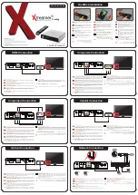
CABINET DISASSEMBLY INSTRUCTIONS . . . . . . . . . . . . . . . . . . . . . . . . . . . . . . . . . . . . . . . . . . . . . . . . . . .1-6-1

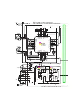
BLOCK DIAGRAMS . . . . . . . . . . . . . . . . . . . . . . . . . . . . . . . . . . . . . . . . . . . . . . . . . . . . . . . . . . . . . . . . . . . . . .1-7-1

SCHEMATIC DIAGRAMS / CBA'S AND TEST POINTS . . . . . . . . . . . . . . . . . . . . . . . . . . . . . . . . . . . . . . . . . .1-8-1

WAVEFORMS  . . . . . . . . . . . . . . . . . . . . . . . . . . . . . . . . . . . . . . . . . . . . . . . . . . . . . . . . . . . . . . . . . . . . . . . . . .1-9-1

WIRING DIAGRAM  . . . . . . . . . . . . . . . . . . . . . . . . . . . . . . . . . . . . . . . . . . . . . . . . . . . . . . . . . . . . . . . . . . . . .1-10-1

FIRMWARE RENEWAL MODE . . . . . . . . . . . . . . . . . . . . . . . . . . . . . . . . . . . . . . . . . . . . . . . . . . . . . . . . . . . .1-11-1

SYSTEM CONTROL TIMING CHARTS. . . . . . . . . . . . . . . . . . . . . . . . . . . . . . . . . . . . . . . . . . . . . . . . . . . . . .1-12-1

IC PIN FUNCTION DESCRIPTIONS . . . . . . . . . . . . . . . . . . . . . . . . . . . . . . . . . . . . . . . . . . . . . . . . . . . . . . . .1-13-1

LEAD IDENTIFICATIO . . . . . . . . . . . . . . . . . . . . . . . . . . . . . . . . . . . . . . . . . . . . . . . . . . . . . . . . . . . . . . . . . . .1-14-1

EXPLODED VIEWS . . . . . . . . . . . . . . . . . . . . . . . . . . . . . . . . . . . . . . . . . . . . . . . . . . . . . . . . . . . . . . . . . . . . .1-15-1

MECHANICAL PARTS LIST  . . . . . . . . . . . . . . . . . . . . . . . . . . . . . . . . . . . . . . . . . . . . . . . . . . . . . . . . . . . . . .1-16-1

ELECTRICAL PARTS LIST . . . . . . . . . . . . . . . . . . . . . . . . . . . . . . . . . . . . . . . . . . . . . . . . . . . . . . . . . . . . . . .1-17-1

MITSUBISHI DIGITAL ELECTRONICS AMERICA, INC.

9351 Jeronimo Road, Irvine, CA  92618-1904

Copyright  ©  200

2

  Mitsubishi Digital Electronics America, Inc.

All Rights Reserved

Summary of Contents for DD-4030

Page 1: ...S 1 6 1 BLOCK DIAGRAMS 1 7 1 SCHEMATIC DIAGRAMS CBA S AND TEST POINTS 1 8 1 WAVEFORMS 1 9 1 WIRING DIAGRAM 1 10 1 FIRMWARE RENEWAL MODE 1 11 1 SYSTEM CONTROL TIMING CHARTS 1 12 1 IC PIN FUNCTION DESCRIPTIONS 1 13 1 LEAD IDENTIFICATIO 1 14 1 EXPLODED VIEWS 1 15 1 MECHANICAL PARTS LIST 1 16 1 ELECTRICAL PARTS LIST 1 17 1 MITSUBISHI DIGITAL ELECTRONICS AMERICA INC 9351 Jeronimo Road Irvine CA 92618 1...

Page 2: ...Manufactured under license from Dolby Laboratories Dolby and the double D symbol are trademarks of Dolby Laboratories DTS and DTS Digital Out are trademarks of Digital Theater Systems Inc ...

Page 3: ...ly AC120 V 60 Hz 3 Load imp 100 K ohm 4 Room ambient 25 C ITEM CONDITIONS UNIT NOMINAL LIMIT 1 Video Output 75 ohm load Vpp 1 0 2 Coaxial Digital Out mVpp 500 3 Audio PCM 3 1 Output Level 1kHz 0dB Vrms 2 0 3 2 S N dB 110 3 3 Freq Response DVD fs 48kHz 20 22kHz dB 2 CD fs 44 1kHz 20 20 kHz dB 2 3 4 THD N 1 kHz 0dB 0 005 ...

Page 4: ...tion shown in the figure When checking the laser diode be sure to keep your eyes at least 30cm away from the pickup lens when the diode is turned on Do not look directly at the laser beam Caution Use of controls and adjustments or doing procedures other than those specified herein may result in hazardous radiation exposure Do not look directly at the laser beam coming from the pickup or allow it t...

Page 5: ...especially 1 Wires covered with PVC tubing 2 Double insulated wires 3 High voltage leads D Use specified insulating materials for hazardous live parts Note especially 1 Insulation tape 2 PVC tubing 3 Spacers 4 Insulators for transistors E When replacing AC primary side components transformers power cord etc wrap ends of wires securely about the terminals before solder ing F Observe that the wires ...

Page 6: ...ference only Be sure to confirm the precise values 2 Leakage Current Test Confirm the specified or lower leakage current between B earth ground power cord plug prongs and externally exposed accessible parts RF termi nals antenna terminals video and audio input and output terminals microphone jacks earphone jacks etc is lower than or equal to the specified value in the table below Measuring Method ...

Page 7: ...ve the flat pack IC with tweezers while apply ing the hot air 3 Bottom of the flat pack IC is fixed with glue to the CBA when removing entire flat pack IC first apply soldering iron to center of the flat pack IC and heat up Then remove glue will be melted Fig S 1 6 1 Release the flat pack IC from the CBA using twee zers Fig S 1 6 Caution 1 Do not supply hot air to the chip parts around the flat pa...

Page 8: ...l pins of the flat pack IC you can remove it easily Fig S 1 3 2 Affix the wire to a workbench or solid mounting point as shown in Fig S 1 5 3 While heating the pins using a fine tip soldering iron or hot air blower pull up the wire as the solder melts so as to lift the IC leads from the CBA contact pads as shown in Fig S 1 5 4 Bottom of the flat pack IC is fixed with glue to the CBA when removing ...

Page 9: ...ur due to a potential difference caused by electro static charge during unpacking or repair work 1 Ground for Human Body Be sure to wear a grounding band 1MΩ that is prop erly grounded to remove any static electricity that may be charged on the body 2 Ground for Workbench 4 Be sure to place a conductive sheet or copper plate with proper grounding 1MΩ on the workbench or other surface where the sem...

Page 10: ...ER Button Press to accept a setting 14 ZOOM Button Enlarges part of a DVD reproduced image 15 REV Button Fast reverse playback to a desired point 16 SEARCH MODE Button Press to locate a desired point 17 REPEAT Button Repeats playback of the current disc title chapter or track 18 MODE Button Activates program playback or random playback mode when playing CDs or MP3 Also Sets Black level 19 DIMMER B...

Page 11: ... the repeat mode is set Lights up when the multi angle scene is taken Displays a chapter or track number Displays a title number Displays the disc status Displays the time lapse of the current title or track Power on Power off Tray open and closed LOAD No disc or error During playback During pause Stop Resume ON Stop Resume OFF ERROR ON is lit Disc icon is lit OFF is lit ERROR is lit Disc icon bli...

Page 12: ...t release two Locking Tabs A at the side and then three Locking Tabs B at the bottom CAUTION 2 Electrostatic breakdown of the laser diode in the optical system block may occur as a potential difference caused by electrostatic charge accumulated on cloth human body etc during unpacking or repair work To avoid damage of pickup follow next procedures 2 1 Slide out the pickup unit as shown in Fig D4 2...

Page 13: ...ront Assembly Tray Panel Fig D2 S 3 CN101 CN401 CN2001 L 4 L 4 S 2 5 DVD Mecha 4 PCB Holder 3 Function CBA Fig D3 View for B Pickup Unit C B Short the three short lands by soldering View for C Slide View for A OR Short the three short lands by soldering DVD Mecha A Fig D4 ...

Page 14: ...ay Top Case S 7 L 5 S 5 S 6 S 5 CN1601 CN1001 S 6 S 4 7 DVD Main CBA Unit 6 AV CBA Fig D5 S 6 8 Rear Panel Fig D6 HOW TO MANUAL EJECT 1 Remove the Top Case 2 Insert the eject bar length approximately 80 mm diameter approximately 3 mm into the manual eject hole on the DVD Mecha Then press it until the tray is ejected ...

Page 15: ...e K1 K2 FP STB FP DIN FP DOUT FP CLK GRID FIP SEGMENT FL2001 IC2003 DVD MAIN CBA UNIT AV CBA SWITCH CBA FG CBA RELAY CBA FRONT PANEL CONTROL BLOCK DIAGRAMS TREV TIN TOUT TFWD MUTE PS CD DVD CFE CAS STANDBY ADDRESS BUS DATA BUS CD DVD CFE CAS STANDBY 71 62 63 70 SCK 72 STDIO SEN SCK STDIO 20 21 22 10 11 FG SENSOR CN401 FP STB 21 21 FP DIN 22 22 FP DOUT 23 23 FP CLK 24 24 REMOTE 26 26 14 80 2 4 IC10...

Page 16: ...ACKING MOTOR DRIVE LOADING MOTOR DRIVE SPINDLE MOTOR DRIVE POWER SAVE SLIDE MOTOR DRIVE LOADING MOTOR SPINDLE MOTOR SLIDE MOTOR M 5 21 2 1 23 26 25 27 22 24 4 67 115 114 118 117 DVD MAIN CBA UNIT FROM TO SYSTEM CONTROL BLOCK DIAGRAM FROM TO DVD SIGNAL PROCESS BLOCK DIAGRAM SCK CD DVD TESTSG ARF NARF STDIO SEN 11 STANDBY TRAY IN 3 GND 5 TRAY OUT 4 TRAY IN TRAY OUT DAC1 DAC0 TRSDRV 119 DATA VIDEO AU...

Page 17: ...A SLICER PLL VCO CPU INTERFACE VIDEO AUDIO INTERFACE DVD DEMODULATOR MEMORY MANAGER 172 168 166 164 160 158 151 149 82 TO VIDEO BLOCK DIAGRAM BCA DATA VIDEO AUDIO SIGNAL DVD MAIN CBA UNIT FROM TO SYSTEM CONTROL BLOCK DIAGRAM CPUDT0 NINT1 ADDRESS BUS DATA BUS NINT2 NINT1 NINT2 WAIT RE WEL CS1 RESET WAIT RE WEL CS1 RESET CPUDT7 30 22 17 9 44 37 CPUADR0 CPUADR17 2 5 6 36 35 34 47 OSCI1 X201 16 9344MH...

Page 18: ...S 58 63 66 73 74 19 CS CS INTERNAL PERIPHERALS PORTS PROGRAMMABLE CPU INTERFACE CENTRAL COMMAND PORT FRONT END LINK INTERFACE ST20 ARBITER MEMORY CONTROLLER SDRAM ARBITER SHARED SDRAM INTERFACE I F VIDEO DECODER AUDIO DECODER CACHE SUBSYSTEM CPU VIDEO FILTERING OSD SP DECODER MIXING 4dB AMP 2dB AMP LPF DRIVER Y C CD FIFO SDRAM BLOCK MOVE DENC SPDIF PCM LRCLK PCM SCLK PCM DATA0 PCM BCK FROM DVD SIG...

Page 19: ...UT 1 2 3 13 14 15 16 FROM VIDEO BLOCK DIAGRAM SERIAL PORT SERIAL CONTROL 4X 8X OVERSAMPLING DIGITAL FILTER FUNCTION CONTROLLER ENPHANCED MULTI LEVEL DELTA SIGMA MODULATOR DAC LPF AMP L CH R CH LPF AMP DAC ZERO DETECT SYSTEM CLOCK 1 2 6 7 5 AUDIO R OUT PCM BCK SPDIF PCM DATA0 PCM LRCLK ADAC MD ADAC MC ADAC ML PCM SCLK AV CBA DVD MAIN CBA UNIT AUDIO SIGNAL DATA AUDIO SIGNAL 18 18 SPDIF A MUTE 3 3V Q...

Page 20: ... ON 3 3V P ON 12V EV 5V IC1006 SHUNT REGULATOR SWITCHING D1008 D1030 RECTIFIER D1003 RECTIFIER D1009 RECTIFIER D1013 D1016 RECTIFIER SWITCHING CONTROL LATCH REG 1 2 6 BRIDGE RECTIFIER HOT AV CBA REPLACE FUSE AS MARKED Ce symbole reprèsente un fusible à fusion rapide CAUTION FOR CONTINUED PROTECTION AGAINST FIRE HAZARD REPLACE ONLY WITH THE SAME TYPE FUSE ATTENTION POUR UNE PROTECTION CONTINUE LES ...

Page 21: ...identified by the mark in the schematic diagram and the parts list Before replacing any of these components read the parts list in this manual carefully The use of substitute replacement parts that do not have the same safety characteristics as speci fied in the parts list may create shock fire or other hazards Capacitor Temperature Markings Capacitors and transistors are represented by the fol lo...

Page 22: ...aintain original function and reliability of repaired units use only original replacement parts which are listed with their part numbers in the parts list section of the service manual 4 Wire Connectors 1 Prefix symbol CN means connector can disconnect and reconnect 2 Prefix symbol CL means wire solder holes of the PCB wire is soldered directly 5 Mode SP 6 Voltage indications for PLAY mode on the ...

Page 23: ...1 8 3 1 8 4 1 8 5 E5640SCD1 DVD Main 1 4 Schematic Diagram ...

Page 24: ...DVD Main 2 4 Schematic Diagram 1 8 6 1 8 7 1 8 8 E5640SCD2 ...

Page 25: ...DVD Main 3 4 Schematic Diagram 1 8 9 1 8 10 1 8 11 E5640SCD3 ...

Page 26: ...components in the power supply circuit are not defective before you connect the AC plug to the AC power supply Otherwise it may cause some components in the power supply circuit to fail CAUTION FOR CONTINUED PROTECTION AGAINST FIRE HAZARD REPLACE ONLY WITH THE SAME TYPE FUSE ATTENTION POUR UNE PROTECTION CONTINUE LES RISQES D INCELE N UTILISER QUE DES FUSIBLE DE MEMO TYPE RISK OF FIRE REPLACE FUSE...

Page 27: ...AV 2 3 Schematic Diagram 1 8 15 1 8 16 E5640SCAV2 ...

Page 28: ...PBC CD VIDEO DVD B CHP 9G TTL TRK 10G 11G A a d g h i j c b e f 11G 9G 10G 8G 7G 6G 5G 4G 3G 2G 1G a b c d e f g c d e f g h i j c d e f g c d e f g c d e f g h i c d e f g c d e f g c d e f g c d e f g c d e f g c d e f g h i j a b a b c d e f g a b a b a b a b a b a b a b a b a b FL2001 MATRIX CHART TRK TTL DVD VIDEO CD PBC CHP A B ...

Page 29: ...SENT IN THE POWER SUPPLY CIRCUIT AN ISOLATION TRANSFORMER MUST BE USED ALSO IN ORDER TO HAVE THE ABILITY TO INCREASE THE INPUT SLOWLY WHEN TROUBLESHOOTING THIS TYPE POWER SUPPLY CIRCUIT A VARIABLE ISOLATION TRANSFORMER IS REQUIRED CAUTION FOR CONTINUED PROTECTION AGAINST FIRE HAZARD REPLACE ONLY WITH THE SAME TYPE FUSE ATTENTION POUR UNE PROTECTION CONTINUE LES RISQES D INCELE N UTILISER QUE DES F...

Page 30: ...BECAUSE A HOT CHASSIS GROUND IS PRESENT IN THE POWER SUPPLY CIRCUIT AN ISOLATION TRANSFORMER MUST BE USED ALSO IN ORDER TO HAVE THE ABILITY TO INCREASE THE INPUT SLOWLY WHEN TROUBLESHOOTING THIS TYPE POWER SUPPLY CIRCUIT A VARIABLE ISOLATION TRANSFORMER IS REQUIRED CAUTION FOR CONTINUED PROTECTION AGAINST FIRE HAZARD REPLACE ONLY WITH THE SAME TYPE FUSE ATTENTION POUR UNE PROTECTION CONTINUE LES R...

Page 31: ...Function CBA Top View Function CBA Bottom View 1 8 23 1 8 24 BE5641F01021 ...

Page 32: ...TOP MODE WF1 WF3 WAVEFORMS WF6 SPDIF Pin 18 of CN1601 1V 0 2usec WF1 Pin 5 of CN1601 WF3 Pin 9 of CN1601 WF4 AUDIO L Pin 13 of CN1601 1V 0 5msec WF5 AUDIO R Pin 15 of CN1601 1V 0 5msec WF2 Pin 7 of CN1601 VIDEO Y 0 2V 20usec VIDEO CVBS 0 5V 20usec VIDEO C 0 2V 20usec ...

Page 33: ... 23 23 FP CLK 24 24 CN501 CN1001 CN2001 CN2041 VIDEO V 1 1 K2 1 1 KEY 2 2 2 NU 3 3 GND 4 4 NU 2 2 VIDEO U 3 3 GND 4 4 VIDEO Y 5 5 A L MUTE 12 12 GND 11 11 GND 6 6 VIDEO CVBS 7 7 GND 8 8 VIDEO C 9 9 GND 10 10 CN701 CN1601 JP1003 JP1004 AC CORD AUDIO OUT L AUDIO OUT R VIDEO OUT DIGITAL AUDIO OUT S VIDEO OUT EV 2 5V 3 3 KEY 4 1 1 KEY 3 2 2 KEY 2 3 3 KEY 1 4 4 K2 5 5 K1 6 6 25 25 26 26 OC KEY REMOTE C...

Page 34: ... in 2 of Fig c is described as follows 5 After programming is finished the tray opens auto matically Fig e appears on the screen and the checksum in 3 of Fig e appears on the VFD Fig f At this time no buttons are available 6 For tray opening plug the AC cord into the AC out let 7 Turn the power on by pressing the power button and the tray will close BE F W VERSION UP MODE PLEASE INSERT A DISC FOR ...

Page 35: ...1 LM LM I o TL123 SP TP122 Tv TL122 0V 5V 0V Tray close Tray open Tray close Play Play Tray open Play 0V Eject key on 6V 2V 5V 0V Disc Rotation Eject key on 2V 2 0s 0V 6V 4 4s 1 2s 700ms 1 7s 0V SYSTEM CONTROL TIMING CHARTS ...

Page 36: ...1 Segment Output Key Souce 1 15 Out b Key 2 Segment Output Key Souce 2 16 Out c Key 3 Segment Output Key Souce 3 17 Out d Key 4 Segment Output Key Souce 4 18 OUT e Display Segment 19 OUT f Display Segment 20 OUT g Display Segment 21 OUT h Display Segment 22 OUT i Display Segment 23 OUT j Display Segment 24 N U Not Used 25 N U Not Used 26 N U Not Used 27 N U Not Used 28 N U Not Used 29 N U Not Used...

Page 37: ... E C B 2SA1015 Y TPE2 KTA1266 Y 2SA966 Y 2SC2236 Y TPE6 C E C B 2SC2785 H KTC3199 GR KRA110M KTA1273 Y KRC110M AT BA1L3Z T BN1L3Z P KTC3205 Y A K C E LTV 817 B C F R A K KIA431 AT G D S 2SK3374 1 2 3 4 PQ018EF01SZ 34 18 17 MM1567AJ MM1566AF 1 GP1FA512TZV 0C 0805T 002 1 2 3 33 23 11 12 21 44 34 PT6315 1 LEAD IDENTIFICATIONS ...

Page 38: ...1 2L071 2L071 2L011 2L011 2L011 A2 A16 2L021 2L031 2L021 A15 A17 F1001 AC1001 2L041 2L041 1B1 2L031 A26 A1X 2B4 A13 A13 IC1204 2L031 2L051 2B2 2B5 2L081 2L021 DVD Main CBA Unit Function CBA AV CBA See Electrical Parts List for parts with this mark Some Ref Numbers are not in sequence Switch CBA ...

Page 39: ...1 15 2 E5640EX X10 X5 X2 X4 S2 S2 S4 Unit S1 A22 A30 A22 A30 X1 X31 S7 Packing ...

Page 40: ...art Number OWNERS GUIDE I B DD4030 REMOTE NA010UD PCB AV OVSA12864 PCB FUNCTION OVSA12867 PCB MAIN N79MOFUP I R RECEIVER USESJRSKK037 MECHA PU N79F1FVM FRONT ASSY OVM203663 COVER TOP OVM101038 DD 4030 Parts List Parts List ...

Reviews: