background image

SERVICE MANUAL

Performance Specifications ................................... 2 - 3
Notes ......................................................................... 3
Rear Panel .................................................................. 4
Section Location ........................................................ 4
Block Diagram ...................................................... 5 - 7
Interconnection Diagram .................................... 8 - 10
Display Schematic and PCB ............................... 11 - 18
Keyboard Schematic and PCB ....................... 13, 17 - 18
Bottom Schematic and PCB ................................ 19 - 24
Power Supply Schematic and PCB ..................... 25 - 28
Data2 Schematic and PCB ................................. 29 - 32
Data1 Schematic and PCB ................................. 33 - 36

Digital Schematic and PCB ................................ 37 - 40
S-Video Schematic and PCB .............................. 41 - 52
Composite Video Schematic and PCB ............... 53 - 58
Main Audio Schematic and PCB ....................... 59 - 74
Multi Channel Schematic and PCB .................... 75 - 86
Amplifier Schematic and PCB .......................... 89 - 104
Tuner AM/FM Alignment  Procedure ............. 105 - 106
Tuner/RAA1 Schematic and PCB ................... 107 - 110
DSP Module PCB ................................................... 111
Backup Power Supply ............................................ 112
Exploded Views and Parts Lists ...................... 113 - 114
Repacking Instruction ............................................ 115

CONTENTS

A/V SYSTEM CONTROLLER

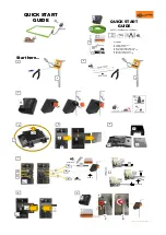
Summary of Contents for MHT200

Page 1: ...hematic and PCB 29 32 Data1 Schematic and PCB 33 36 Digital Schematic and PCB 37 40 S Video Schematic and PCB 41 52 Composite Video Schematic and PCB 53 58 Main Audio Schematic and PCB 59 74 Multi Channel Schematic and PCB 75 86 Amplifier Schematic and PCB 89 104 Tuner AM FM Alignment Procedure 105 106 Tuner RAA1 Schematic and PCB 107 110 DSP Module PCB 111 Backup Power Supply 112 Exploded Views a...

Page 2: ...ossover Setting Power Amplifier Specifications Power Output Minimum sine wave continuous average power output per channel all channels operating is 100 watts into 4 ohm load 70 watts into a 8 ohm load Rated Power Band 20Hz to 20 000Hz Total Harmonic Distortion Maximum Total Harmonic Distortion at any power level from 250 milliwatts to rated power output is 0 05 for 4 or 8 ohm load Dynamic Headroom...

Page 3: ...h is 15uV across 75 ohms Signal To Noise Ratio Mono 75dB Stereo 70dB Frequency Response Mono 0 1dB from 20Hz to 15 000Hx Stereo 0 1dB from 20Hz to 15 000Hz Harmonic Distortion Mono 0 3 at 100Hz 0 3 at 1 000Hz 0 3 at 10 000Hz Stereo 0 45 at 100Hz 0 45 at 1 000Hz 0 65 at 10 000Hz Intermodulation Distortion Mono 0 25 Stereo 0 45 Capture Ratio 1 2dB Alternate Channel Selectivity 75dB Spurious Response...

Page 4: ...ONAL 5 DATA2 PCB 3 BOTTOM PCB 4 POWER SUPPLY PCB 2B KEYBOARD PCB 7 DIGITAL PCB 8 S VIDEO PCB 10 MAIN PCB 12B AMP PCB BACK 12A AMP PCB FRONT 2A DISPLAY PCB 11 MULTI CHANNEL PCB 15 DSP MODULE 16 BACKUP POWER SUPPLY PCB 14 RAA1 RAA1 14 15 16 SEE INTERCONNECT TOP VIEW WITH COVER REMOVED ...

Page 5: ...UT MUTING LEFT RIGHT ZB OUTPUT DSP EXT PROCESSOR SWITCHING L C R SUB SL SR BSL BSR L C R SUB SL SR BSL BSR L C R SUB LS RS BSL BSR 8 CHANNEL D A DIFF AMP VOLUME AMP PREDRIVER DRIVER OUTPUT POWER GUARD GAIN ELECTRONIC ATTENUATOR PG INDICATOR DRIVER PG INDICATOR CURRENT SOURCE DC BIAS DIFF AMP VOLUME AMP PREDRIVER DRIVER OUTPUT NEGATIVE CURRENT LIMITER POSITIVE CURRENT LIMITER NEGATIVE FEEDBACK DC S...

Page 6: ...HP_R FIL1 12V GND 15A JACKSW GND BULB2 BULB2 BULB2 FIL2 29V GND 15A GND GND HP_L GND 1 40 MAIN_LB JACKSW HP_R MAIN_L MAIN_C MAIN_R MAIN_LS MAIN_RS MAIN_RB 5VA CHANNEL10_BB GND HP_L GND GND GND CHANNEL9_BB GND AMP_Z_R AMP_Z_L SCLK 15A MUTEMAIN RESET OUT2 OUT1 MOSI IN1 MAIN_SW GND GND GND GND INTERRUPT3 GND GND OUT3 5D SLOT_SELECT3 FIL1 POWER CTRL BULB2 BULB1 FIL2 CENTER DELAY DRIVE 15V 29V 15A 12 3...

Page 7: ...C 14 GND 7 IC5A 74HC74 1 2 clockwise 2 Counterclockwise R90 120k detent click Rotary PRE 4 CLK 3 D 2 CLR 1 VCC GND IC7A 74HC74 ClearInt C52 100uF 5D C40 100uF 5D C54 3n3 C55 3n3 detent C20 100uF 5D C42 100uF 5D 5D 5D LatchIn ClearInt TP2 1 CCW 3 CW case ROT1 5D 1 CCW 3 CW case ROT3 1 CCW 3 CW case ROT2 5D 5D D8 LL4148 D7 LL4148 D26 LL4148 D24 LL4148 D6 LL4148 D5 LL4148 C8 100n C7 100n C5 100n C4 1...

Page 8: ...L 13 SEGK 14 SEGJ 15 SEGI 16 VEE 17 SEGH 18 SEGG 19 SEGF 20 SEGE 21 SEGD 22 SEGC 23 SEGB 24 SEGA 25 SCLK 26 DATA IN 27 LOAD 28 OSCI 29 OSCO 30 POR 31 VDD 32 IC9 MSC7112 01 DS6 DS5 DS2 DS1 DS3 DS4 DS8 DS10 DS7 DS9 Light bulbs Bulb1 Bulb2 29V 11 12 13 IC8D 74HC02 VFD_Load VFD_Load VFD_data_En VFD_data_En Bulb1 Bulb2 Fil1 Fil2 15A 15A JackSw 12V HP_R HP_L MH3 MH1 MH2 MH4 Mounting holes MH5 MH6 MH1 MH...

Page 9: ... MOLDfor selectorleds M10 MOLDfor selectorleds M11 LED27 LED28 LED30 LED32 LED31 LED29 NOTE LEDbars need socket strips e g SAMTEC CES 110 01 T S 3 4 5 6 7 8 1 2 X18 X8P2M R104 560R R105 560R R106 560R A 1 K 3 E 4 C 6 IC12 TLP127 Toshiba R107 240R Standoff for led E7 Standoff for led E8 Standoff for led E9 DTS DTS DTS ES DTS ES ProLogic ProLogic DD EX DD PGuard PGuard R117 300R R118 not installed R...

Page 10: ...115 100k C66 10p 15A_2 R113 100k R114 100k C65 100n C64 100n 15A_2 15A_2 3 2 1 8 4 IC21A TL072 1 2 X21 Not Installed C63 10u Mic d 4 3 1 2 X9 AD Electronics 3052 40 4 3 1 2 R50 22k X3 R51 1M D12 LL4148 D14 LL4148 5D_2 5D_2 JackSwd HP_Ld HP_Rd 1 2 3 4 X4 X4F1M HP_Rd HP_Ld JackSwd not installed AD Electronics 3052 40 ...

Page 11: ...4 5 6 X1 1x6 Molex connector 5 5 gnd gnd 15 15 Bulb1 R13 390k R11 180k C35 10u 13 11 9 4 6 8 1 16 RE1 NotInstalled 15A 15A 15A_amp 15A_amp 5Va 2 3 1 Q2 BC858 2 3 1 Q3 BC858 3 2 1 Q4 BC848 15A_amp 15A_amp R12 NotInstalled C36 NotInstalled Bulb1 Option1 Option2 D2 NotInstalled D1 NotInstalled DelayDrive DelayDrive OptionalRelayfor 15V R1 NotInstalled R6 NotInstalled R16 NotInstalled AGND VGND C3 10u...

Page 12: ... 21 23 25 22 24 26 27 28 29 30 31 32 33 34 35 36 37 38 39 40 X17 X40P2M ENA_VIDEO CsVIDEO_TO_OUTBUF CsVIDEO_SW_OUT SEL_0 OE_0 reset 5D Interrupt2 5Va 5Va MOSI MISO SCLK Out1 Out2 Out3 In1 slot_select2 L10 Ferrite bead L9 Ferrite bead L11 Ferrite bead 3 4 5 6 7 8 9 10 11 12 14 13 1 2 15 16 18 17 19 20 21 23 25 22 24 26 27 28 29 30 31 32 33 34 35 36 37 38 39 40 X18 X40P2M VIDEO_SCLK LATCH_SEL ENA_VI...

Page 13: ...BOTTOM 320168 3 23 24 MHT200 ...

Page 14: ...POWER SUPPLY 320131 25 26 4 500mA 1 6A F1 T1 6AL 250V F2 T500mAL 250V ...

Page 15: ...POWER SUPPLY 320131 4 27 28 MHT200 ...

Page 16: ...ges between 5V and 8V If Power A B is at 0V then at 5V L1 NFM51R10P157 C29 10u R30 75R 5A R31 100k L2 NFM51R10P157 C30 10u R34 75R 5A R36 100k L4 NFM51R10P157 C31 10u R35 75R 5A R37 100k L6 NFM51R10P157 C32 10u R38 75R 5A R39 100k L7 NFM51R10P157 C33 10u R41 75R 5A R42 100k L9 NFM51R10P157 C34 10u R44 75R 5A R45 100k IN1R IN1G IN1B IN2R IN2G IN2B OUTR OUTB OUTG R4775R R4675R R48 75R OUTR OUTG OUTB...

Page 17: ...DATA2 320123 5 31 32 MHT200 ...

Page 18: ...DATA1 320122 6 33 34 ...

Page 19: ...DATA1 320122 6 35 36 MHT200 ...

Page 20: ... nc 4 5 6 nc 8 TR1 input0 input1 input2 2 1 KP1 2 1 KP2 2 1 KP3 2 1 KP4 C4 Not Installed DigitalOutput R8 0R R21 0R R23 0R R25 0R R24 0R R22 0R TxD_BBconn RxD_BBconn Vcc 16 T1Out 14 R1In 13 T2Out 7 R2In 8 R1Out 12 R2Out 9 T1In 11 T2In 10 C1 1 C1 3 C2 4 C2 5 V 2 V 6 GND 15 IC5 MAX232CSE R4 75R R5 75R R11 10k 1 6 2 7 3 8 4 9 5 X4 ITW McMurdo SDES9SN R20 0R RS 232 driver C17 100n C29 1u C28 1u C31 1u...

Page 21: ...DIGITAL 320126 7 39 40 MHT200 ...

Page 22: ...S VIDEO 320125 SH 1 OF 5 8 41 42 ...

Page 23: ...S VIDEO 320125 SH 2 OF 5 43 44 MHT200 8 ...

Page 24: ...S VIDEO 320125 SH 3 OF 5 8 45 46 ...

Page 25: ...S VIDEO 320125 SH 4 OF 5 8 47 48 MHT200 ...

Page 26: ...S VIDEO 320125 SH 5 OF 5 8 49 50 ...

Page 27: ...S VIDEO 320125 8 51 52 MHT200 ...

Page 28: ...COMPOSITE VIDEO 320124 SH 1 OF 2 9 53 54 ...

Page 29: ...COMPOSITE VIDEO 320124 SH 2 OF 2 9 55 56 MHT200 ...

Page 30: ...COMPOSITE VIDEO 320124 9 57 58 ...

Page 31: ...d C30 Not Installed 15A 5 6 7 IC12B TL072 R102 20k R100 20k C95 33p R27 100k C50 10u C51 10u 1 2 3 4 5 6 Shield 7 X2 HSP 244V4 17 1 2 3 4 5 6 Shield 7 X5 HSP 244V4 17 1 2 3 4 5 6 Shield 7 X6 HSP 244V4 17 TunerL TunerR 2 1 KP1 2 1 KP2 2 1 KP3 2 1 KP4 2 1 KP9 2 1 KP10 2 1 KP11 2 1 KP12 2 1 KP13 2 1 KP14 2 1 KP15 2 1 KP16 15A 15A C126 100n C128 100n C129 100n C130 100n C236 10u C238 10u 3 2 1 8 4 IC1...

Page 32: ... Installed C242 10u 16V R219 Not Installed R54 Not Installed R220 Not Installed R232 0R 2 6 1 Q7A Not Installed 5 3 4 Q7B Not Installed R213 56R ZoneB_R ZoneB_L VCR2_R VCR2_L MuteTrB C265 Not Installed C264 Not Installed 3 2 1 8 4 IC18A TL072 15A R60 100k R58 100k C100 33p 15A 5 6 7 IC18B TL072 R64 100k R63 100k C101 33p R216 56R C243 10u 16V R221 Not Installed R61 Not Installed R223 Not Installed...

Page 33: ...100k R68 100k C280 22u C279 22u MrSrcSel2 C281 220n C282 220n 3 2 1 8 4 IC19A TL072 5 6 7 IC19B TL072 R182 0R R188 0R VD 7 DGND 11 AGND 16 VA 1 LIN 4 LGND 5 RIN 13 RGND 12 XMUTE 8 XCS 6 DATA 9 CCLK 10 RFO 14 RMO 15 LFO 3 LMO 2 IC48 MAS9116 L17 EXC ML 68R 100MHZ 3A C247 10u C248 10u 5Va 5Va C151 100n C143 100n C142 100n R119 10k 15V 1 GND 12 15V 27 S1a 19 S2a 20 S3a 21 S4a 22 S5a 23 S6a 24 S7a 25 S...

Page 34: ...als R123 10k 5D R140 10k Data write to slot control hw 5D Slot Idenfication data SPI MISO D1 SPI SCK D2 SPI MOSI D3 DGND D4 SPI Sel D5 Out1 D6 HREQ D7 Out2 D8 DGND D9 IC2 D10 reset D11 DGND D12 IC3 D13 TxD D14 IC1 D15 RxD D16 DGND D17 DGND D18 SPDIF In D19 DGND D20 MODULE1A DSP MODULE V5 6 5D C164 100n 2 1 8 VCC 14 GND 7 3 4 5 6 11 12 IC62 74HC30 Read interrupt data Module connector digital SPDIFi...

Page 35: ...5D MuteZoneA PRE 4 CLK 3 D 2 CLR 1 Q 5 Q 6 VCC 14 GND 7 IC14A 74HC74 C5 100n 5D reset 5D Mute2 MuteRec2 Mic_ON SWOut_BBconn COut_BBconn SurOutR_BBconn SurOutL_BBconn MainOutL_BBconn MainOutR_BBconn BackOutR_BBconn BackOutL_BBconn DigInP_BBconn DigInM_BBconn 5Va 5Va 5D 15A 15A 33V MuteMain FP_IRdata IRdata DigitalOK DigitalSelect0 DigitalSelect1 DigitalSelect2 TxD RxD Interrupt0 Interrupt2 slot_sel...

Page 36: ...ner Out1_to_tuner Out2_to_tuner Out3_to_tuner MISO_from_tuner In1_from_tuner R151 10k R152 10k R154 10k R155 10k R156 10k 5D C219 100n L8 EXC ML 68R 100MHZ 3A C278 100u C222 100n C290 22u 5D TunerL TunerR Sclk_to_tuner MOSI_to_tuner PLL_CE TunerMute ScanStop SignalStrength MPXindicator Tuner data Data C224 100n L16 EXC ML 68R 100MHZ 3A C291 4u7 33V REF 1 A_IN 2 REF 3 GND 4 CS 5 D_OUT 6 CLK 7 VCC 8...

Page 37: ... 5 H 6 Qh 7 Qh 9 VCC 16 GND 8 IC57 74HC165 reset IdentClk 5D C229 100n Slot 4 multiroom ID 12 D 14 A 11 SER 10 B 12 C 13 CLK inh 15 SH DL 1 CLK 2 E 3 F 4 G 5 H 6 Qh 7 Qh 9 VCC 16 GND 8 IC52 74HC165 reset IdentClk 5D 5D C223 100n Slot 5 tuner ID 11 D 14 A 11 SER 10 B 12 C 13 CLK inh 15 SH DL 1 CLK 2 E 3 F 4 G 5 H 6 Qh 7 Qh 9 VCC 16 GND 8 IC16 74HC165 reset IdentClk C8 100n Slot 2 videoboard 5D ID 5...

Page 38: ...MAIN AUDIO 320165 10 73 74 X19 TUNER AUX CD SAT TV DVD VCR1 VCR2 ZONEA VCR1 REC VCR2 REC ZONEB DSP MODULE 15 ...

Page 39: ... 10k C77 33p R29 100k LS In 3 2 1 8 4 IC12A TL072 15A R46 20k R42 10k R36 100k C52 Not Installed C69 Not Installed 15A 5 6 7 IC12B TL072 R45 20k R41 10k C79 68p R33 100k R In RS In C In Sw In C1 100p C78 33p C80 150p External 7 1 Inputs 15A 15A C2 100n C12 100n C72 100n C55 100n C73 100n C56 100n R1 0R R2 0R R50 0R R49 0R R52 0R R51 0R C63 10u C64 10u C61 10u C62 10u C13 10u C11 10u 3 2 1 8 4 IC2A...

Page 40: ...D 7 IC32A 74HC74 MuteMain 3 2 1 VCC 14 GND 7 IC33A 74HC02 5 6 4 IC33B 7402 11 12 13 IC33D 7402 8 10 9 IC33C 7402 C204 100u C203 100u C202 100n A 12 B 11 RST 13 Cx 15 Rx Cx 14 Q 10 Q 9 1 IC31B 74HC4538 3 4 5 6 7 8 9 10 11 12 14 13 1 2 15 16 18 17 19 20 21 23 25 22 24 26 27 28 29 30 31 32 33 34 35 36 37 38 39 40 X10 2x20 100mils pinstrip 5Va C205 10u C100 100n C29 100n C28 100n C167 100n 5D bb_Zone_...

Page 41: ...120 20k C144 33p Out_L Out_C Out_R Out_Ls Out_Rs Out_Lb Out_Rb Out_Sw Amp_L Amp_C Amp_R Amp_Ls Amp_Rs Amp_Back Amp_Back Power Amp Connector 1 2 3 4 Shield 6 5 X5 HSP 243V3 48 BP_LOut BP_ROut BP_LSOut BP_RSOut BP_COut BP_SWOut BP_BLOut BP_BROut 1 2 3 Shield 4 X11 HSP 242V3 12 1 2 3 4 Shield 6 5 X6 HSP 243V3 48 1 2 3 4 Shield 6 5 X4 HSP 243V3 48 1 2 3 4 Shield 6 5 X7 HSP 243V3 48 1 2 3 4 Shield 6 5 ...

Page 42: ...6 VA 1 LIN 4 LGND 5 RIN 13 RGND 12 XMUTE 8 XCS 6 DATA 9 CCLK 10 RFO 14 RMO 15 LFO 3 LMO 2 IC16 MAS9116 R48 10R C75 220n C87 220n C90 10u C83 10u L4 BLM31A601S 5Va C88 100n C71 100n C26 100n C192 100n McVolCS1 McVCMute1 McSClk McMosi Center Subwoofer 15A 15A 5 6 7 IC7B OPA2134 5 6 7 IC3B TL072 15A 3 2 1 8 4 IC8A OPA2134 5 6 7 IC8B OPA2134 15A Phones out Out_L Out_C Out_R Out_Sw Vol_L Vol_C Vol_R Vo...

Page 43: ...D 5 RIN 13 RGND 12 XMUTE 8 XCS 6 DATA 9 CCLK 10 RFO 14 RMO 15 LFO 3 LMO 2 IC6 MAS9116 R28 10R C50 220n C51 220n C47 10u C49 10u L2 BLM31A601S R47 10R C70 220n C81 220n C89 10u C59 10u L3 BLM31A601S 5Va 5Va C57 100n C58 100n Out_Ls Out_Rs Out_Lb Out_Rb Vol_Ls Vol_Rs Vol_Lb Vol_Rb 3 2 1 8 4 IC19A TL072 15A 15A 5 6 7 IC19B TL072 R71 20k R72 20k R66 20k R65 20k C125 Not Installed C124 Not Installed Ls...

Page 44: ...MULTI CHANNEL 320169 11 85 86 ...

Page 45: ...NOTES 87 88 MHT200 ...

Page 46: ...AMPLIFIER 320129 FRONT BACK SH 1 OF 7 12A B 89 90 ...

Page 47: ...AMPLIFIER 320129 FRONT BACK SH 2 OF 7 12A B 91 92 MHT200 ...

Page 48: ...AMPLIFIER 320129 FRONT BACK SH 3 OF 7 12A B 93 94 ...

Page 49: ...AMPLIFIER 320129 FRONT BACK SH 4 OF 7 12A B 95 96 MHT200 ...

Page 50: ...AMPLIFIER 320129 FRONT BACK SH 5 OF 7 12A B 97 98 ...

Page 51: ...AMPLIFIER 320129 FRONT BACK SH 6 OF 7 12A B 99 100 MHT200 ...

Page 52: ...AMPLIFIER 320129 FRONT BACK SH 7 OF 7 12A B 101 102 ...

Page 53: ...AMPLIFIER 320129 FRONT BACK 12A B 103 104 MHT200 ...

Page 54: ...n TP1 and TP2 relative connector J6 12 Tune the Generator to 90MHz and adjust the RF Output to 1000uV and 100 MONO modulation at 1000Hz Then adjust T8 FM DETector SECondary for lowest distortion 13 Reduce the Generator Output to minimum and detune the Generator so the Receiver picks up only noise then recheck the voltage between TP1 and TP2 connector J6 Adjust T8 and C65 if needed If it is not 0 0...

Page 55: ...TUNER 049084 13 105 106 107 108 MHT200 ...

Page 56: ...TUNER 049084 13 109 110 RAA1 SECTION 14 NOTE SEE PAGE 105 106 FOR TUNER ALIGNMENT PROCEDURES ...

Page 57: ...1 FLASH IC IC1 133506SP BLANK IC 133507SP MHT200 V6 44 PROGRAMMED IC NOTE BEVELED CORNER TOP REAR PANEL FRONT PANEL SET R1 FOR 5 3VDC AT PIN 2 OF CONNECTOR CN2 5 3VDC R1 LOWER HIGHER 5 3V ADJUSTMENT DSP MODULE 320166 15 BACKUP POWER SUPPLY 320149 16 ...

Page 58: ...8705 EXTRUSIONTOP 19 101172 SCREWTC6 32X1 4PHFLU C 20 094360 TAPE FOAM 1 2 X 1 2 21 004939 BRACKETEXTRUSION 22 018615 ENDCAP9 23 101042 SCREWTS4 40X1 2FILLISTER 24 017738 PLEXIFILTER 25 094017 TAPE FOAM 1 4 X1 4 26 017851 PUSHBUTTONDISPLAYPLEXI 27 017850 PLEXIGLASLOGO TRIM SURROUND 28 101054 SCREWTAPTITE6 32X1 4PHPNBLK 29 005163 TOPCOVER 30 101078 SCREWTAP8 32X5 16PHPNBLK 31 320143 MHT200CONTROLLE...

Page 59: ... securely to the bottom pad and wood skid Failure to do this will result in shipping damage Qty Part No Description 1 033160 Slit scored wrap 1 034198 Inner carton top 1 033725 Top pad 4 017218 Plastic foot unit 1 033739 Poly bag 4 100159 4 104083 1 034197 Bottom pad 2 017218 Plastic foot spacer 1 034196 Shipping skid 2 101169 10 x 2 1 4 Wood screw 2 104033 10 x 1 3 4 Flat washer 2 034159 Foam end...

Page 60: ...ecause of the constant upgrading of McIntosh products circuitry and components the Company cannot insure and does not warrant the accuracy of the within schematic material which is intended for information only McINTOSH LABORATORY INC 2 CHAMBERS STREET BINGHAMTON NEW YORK 13903 Printed in U S A Part Number 040897 A V SYSTEM CONTROLLER SERVICE MANUAL ...

Reviews: