Lattice Semiconductor Smart Socket, User Manual
The Lattice Semiconductor Smart Socket is a cutting-edge device that allows for seamless integration of smart technologies into your home. Enhance your living space with this innovative product. For detailed instructions on how to set up and operate your Smart Socket, download the User Manual for free from manualshive.com.
Share
Download


Reviews:
No comments
Related manuals for Smart Socket
BLUETOOTH KEYBOARD
Brand: Targus Pages: 7

GP68
Brand: B&K Pages: 2
B3
Brand: N-Com Pages: 28

PS5
Brand: CAB Pages: 21

S8
Brand: Baja Designs Pages: 6

176F6516
Brand: Danfoss Pages: 14

Odyssey II Series
Brand: Dakota Digital Pages: 3

modus 600rt
Brand: Hahnel Pages: 176

4832
Brand: Laser Pages: 8

CB-300
Brand: Vello Pages: 8

WP-320 Series
Brand: Waterpik Pages: 2

Breaker ID
Brand: Zircon Pages: 2

StudSensor e50
Brand: Zircon Pages: 1

KN-4530
Brand: Oki Pages: 20
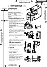
OKO-CENTER 1
Brand: Würth Pages: 2

STEVAL-IOD04KT1
Brand: ST Pages: 13
TERMBOX-1200
Brand: Vaisala Pages: 32

UNIVERSAL 1050
Brand: Jetmaster Pages: 13


